A kind of pcb board soldering method

A technology of PCB board and welding method, which is applied in the field of PCB board processing technology, can solve the problems of wasting PCB board materials and low welding firmness, and achieve the effects of improving aesthetics, increasing tension, and improving production efficiency

Active Publication Date: 2019-12-13
TIANTAI TIANYU OPTOELECTRONIC CO LTD
View PDF1 Cites 0 Cited by
  • Summary
  • Abstract
  • Description
  • Claims
  • Application Information

AI Technical Summary

Problems solved by technology

[0005] The object of the present invention is to provide a PCB board welding method, which solves the defects that the existing PCB board welding method wastes the PCB board material and the welding firmness is not high at the same time

Method used


Image

  • A kind of pcb board soldering method
  • A kind of pcb board soldering method
  • A kind of pcb board soldering method

Examples


Embodiment 1

[0025] Such as figure 1 As shown, a kind of PCB board welding method provided by the present invention comprises:

[0026] a. Move the PCB board from the anti-static bag into the metal plate through the removal device;

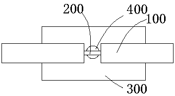
[0027] b. Completely peel off part of the sheath 100 on the wire;

[0028] c. Solder the stripped copper wire 200 on the pad 400 of the PCB 300 .

[0029] Among them, the surface temperature of the welding resistance during welding is lower than 60°C; the total current during welding is 15±1mA; the welding process uses no-cleaning non-conductive flux or no-cleaning non-conductive solder paste.

Embodiment 2

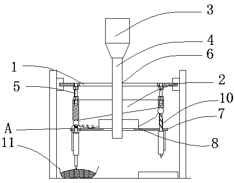
[0031] as attached figure 2 , attached image 3 And attached Figure 4 As shown, the present invention discloses a removal device, which includes an upper fixed plate 1, an arc-shaped cam 2 with an inclined slope, and a rotating shaft 4 connected to a driving motor 3 by transmission at the top, and the cam passes through the fixing member 5. Connect the upper fixing plate; the center of the upper fixing plate is provided with a central hole 6, the rotating shaft is inserted into the central hole, the bottom of the rotating shaft has a lower fixing plate 7, and the middle part of the lower fixing plate is provided with a battery 8; Six fixed sliding holes 9 are evenly installed on the upper circumference of the lower fixed plate; six transfer components 10 are arranged on the outer circumference of the rotating shaft, and an antistatic bag 11 is provided below the lowest point of the transfer component.

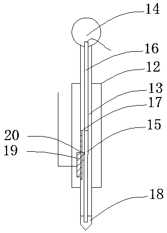
[0032] The removal assembly includes an outer sleeve 12 and a slide ba...


PUM


Abstract

The invention provides a PCB welding method. The PCB welding method comprises the steps of a, completely stripping a sheath on an electric wire; and b, welding the stripped copper wire of the electricwire on a PCB. According to the invention, the sheath on the electric wire is completely stripped without damaging an internal copper wire, and meanwhile, the stripped electric wire sheath is not adhered to the copper wire and does not rebound, so that the welding of the electric wire is not influenced. Parallel connection of the electric wire and a PCB can realize only by designing the conventional bonding pad according to the conventional specification. In this way, the production efficiency can be greatly improved, the product tension is increased, and the attractiveness is improved.

Description

technical field [0001] The invention relates to the field of PCB board processing technology, in particular to a PCB board welding method. Background technique [0002] At present, there are generally two ways to traditionally strip wires and connect wires to the pads of the PCB board. One is that the PCB board needs to be placed with double rows of pads. The wire is connected from the right pad. Another way is to cut the wires, twist the wires together, and then solder them to the PCB pads. The above two methods of stripping and welding, on the one hand, waste PCB board material, and the firmness of welding is not good, which will greatly affect the tensile force and appearance of this product. [0003] For example, as disclosed in the patent document 1: CN201620815367.3, the utility model patent provides a welding structure of a PCB board, including a PCB board, a fixing structure, a pad and a welding post; the pad is arranged on the PCB board , copper skin is laid on t...

Claims


Application Information

Patent Timeline
Patent Type & Authority Patents(China)
IPC IPC(8): H05K3/34
CPCH05K3/34
Inventor 谢克俊
Owner TIANTAI TIANYU OPTOELECTRONIC CO LTD
Why Eureka
Try Eureka