Thin chip vacuum packaging structure
A vacuum packaging and vacuum sealing technology, which is applied in the field of semiconductor manufacturing, can solve the problems of high production cost, large thickness, and large volume, and achieve the effects of reducing volume, meeting miniaturization, and reducing packaging costs
- Summary
- Abstract
- Description
- Claims
- Application Information
AI Technical Summary
Problems solved by technology
Method used
Image
Examples
Embodiment Construction
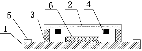
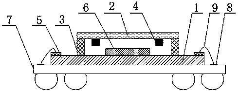
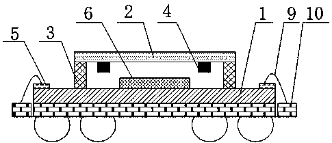
[0022] Combine below figure 1 Referring to FIG. 7 , the embodiment of the present invention and the specific operation process are described in detail, but the scope of protection of the present invention is not limited to the following examples.
[0023] The invention discloses a thin chip vacuum packaging structure, such as figure 1 As shown, it includes a substrate 1, a cover plate 2, a cofferdam 3 and a getter 4, and related circuits are pre-formed on the substrate 1, and the substrate 1, the cover plate 2 and the cofferdam 3 are bonded to form a vacuum sealed cavity body, the substrate 1 is provided with a chip sensing area 6 and a first metal pad 5, the chip sensing area 6 and getter 4 are placed in a vacuum-sealed cavity, and the first metal pad 5 is set on the periphery of the vacuum-sealed cavity.
[0024] In the embodiment of the present invention, the getter 4 is adhered on the cover plate 2, and the getter 4 Activated to absorb the gas released inside the cavity...
PUM
 Abstract
Description
Claims
Application Information
 - R&D
- Intellectual Property
- Life Sciences
- Materials
- Tech Scout
- Unparalleled Data Quality
- Higher Quality Content
- 60% Fewer Hallucinations
Browse by: Latest US Patents, China's latest patents, Technical Efficacy Thesaurus, Application Domain, Technology Topic, Popular Technical Reports.
© 2025 PatSnap. All rights reserved.Legal|Privacy policy|Modern Slavery Act Transparency Statement|Sitemap|About US| Contact US: help@patsnap.com


