
SiP system based on JTAG test and JTAG test method of inside chip of SiP system

A test method and technology of the chip under test, applied in the direction of measuring electricity, measuring devices, measuring electrical variables, etc., can solve the problems of high test plan planning efficiency, complex testing, and various types of functional tests in SiP modules, so as to improve accessibility. , the effect of improving controllability

Inactive Publication Date: 2019-04-02
BEIJING MXTRONICS CORP +1
View PDF7 Cites 3 Cited by
  • Summary
  • Abstract
  • Description
  • Claims
  • Application Information

AI Technical Summary

Problems solved by technology

[0004] The technical solution problem of the present invention is: overcome the weak point of prior art, provide a kind of JTAG test method based on the SiP system of JTAG test and internal chip thereof, be used for realizing the effective test of fully closed or semi-completely closed chip in SiP Functional testing, at the same time, the hardware platform required for testing is simple, and the planning efficiency of testing schemes is high, which optimizes the problems of many types of functional testing and complex testing in SiP modules

Method used


Image

  • SiP system based on JTAG test and JTAG test method of inside chip of SiP system
  • SiP system based on JTAG test and JTAG test method of inside chip of SiP system

Examples


Embodiment Construction

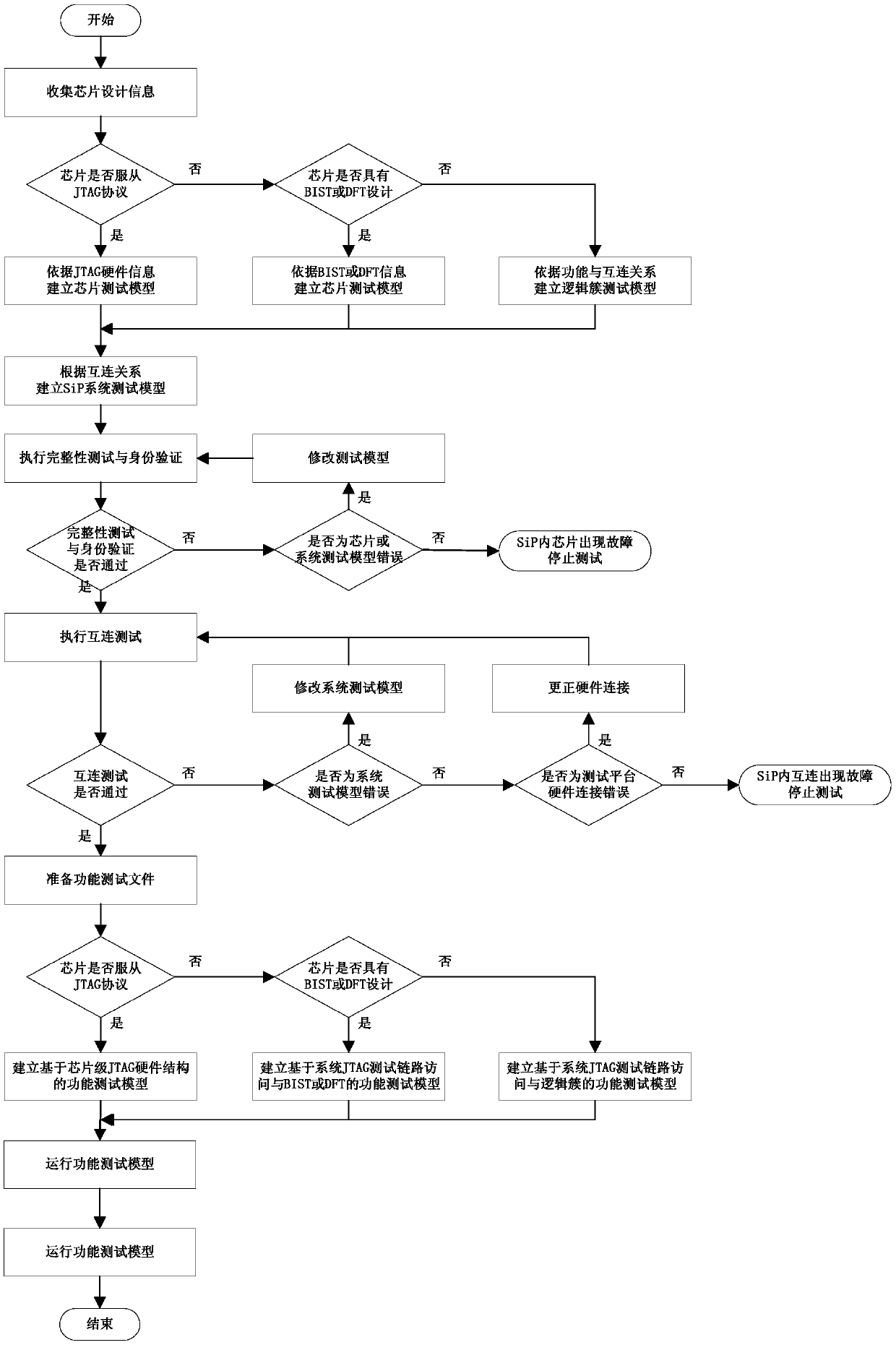
[0026] The present invention will be described in detail below in conjunction with the accompanying drawings and embodiments.

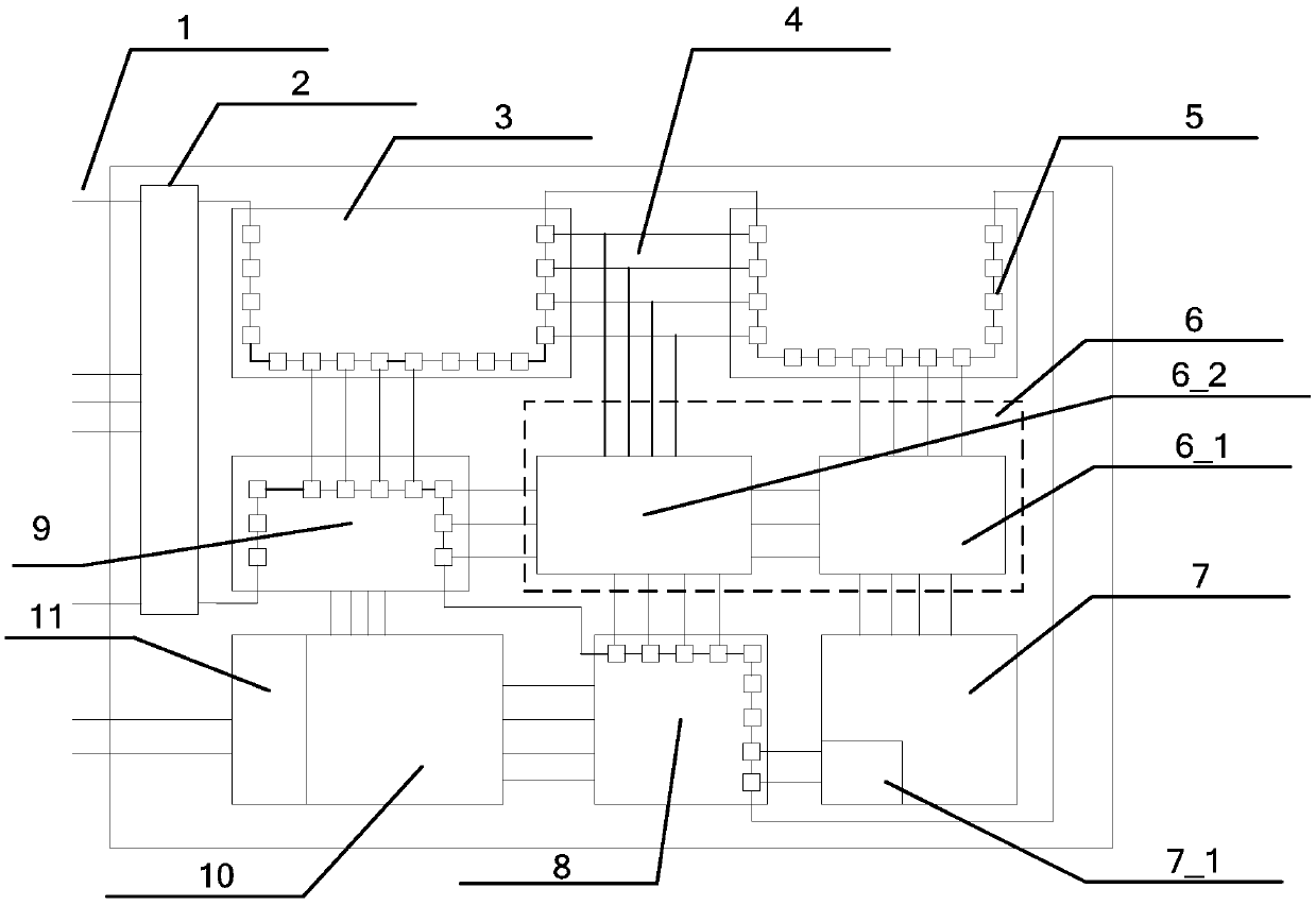
[0027] The invention proposes a JTAG test method for a SiP system based on JTAG test and its internal chips. This method aims at the characteristics that the chip in the SiP module is completely enclosed or semi-completely enclosed in the system package, and realizes the test of the internal chip of the SiP module through the interconnection design of the chip embedded in the SiP module, and uses the boundary scan unit of the chip and the JTAG test port. Implement the data path.

[0028] The SiP system based on JTAG test includes a JTAG test access port, at least two chips subject to the JTAG protocol, which are recorded as the first JTAG chip and the last JTAG chip, and the test input terminal TDI of the JTAG test access port is connected to the JTAG test input of the first JTAG chip On the terminal TDI, the JTAG test output terminal TDO of the firs...


PUM


Abstract

The invention relates to an SiP system based on a JTAG test and a JTAG test method of an inside chip of the SiP system. The SiP comprises a JTAG test access port and at least two chips complying witha JTAG protocol; the at least two chips are recorded as a first JTAG chip and a last JTAG chip; the test input end of the JTAG test access port is connected onto the JTAG test input end of the first JTAG chip; the JTAG test output end of the first JTAG chip is connected with the test input end of the last JTAG chip; the test output end of the last JTAG chip is connected to the test output end of the JTAG test access port; a JTAG test link of the SiP is formed; if other chips to be tested in the SIP are chips complying with the JTAG protocol, the chips are inserted into the JTAG test link of the SIP in a boundary scanning unit interconnection mode; and if other chips are logical clusters or chips not complying with the JTAG protocol, the chips are mutually connected with the boundary scanning unit of the chip complying with the JTAG protocol, and the test data transmission is performed through the JTAG test link of the SIP. The function test data transmission is completed through the JTAG link; and the inside chip test is realized.

Description

technical field [0001] The invention relates to a SiP system based on JTAG testing and an internal chip testing method thereof, and is a testing method which applies board-level JTAG testing technology to SiP module testing for reference. Background technique [0002] System-in-Package (SIP) has developed rapidly in recent years. It is an important way to realize the miniaturization, light weight and multi-function of electronic products, and has become an important advanced packaging and system integration technology. The SIP module integrates different types of circuits (mostly chips (Bare-die), but also chips and discrete components) into the same package, and realizes some passive device functions, interconnection and mechanical functions in high-density interconnected substrates. Installation, and finally complete the functions of the whole or part of the system. The integrated circuits can be of different functions, different processes, and different states, which grea...

Claims


Application Information

Patent Timeline
IPC IPC(8): G01R31/3185
CPCG01R31/318572G01R31/318597
Inventor 秦贺韩逸飞祝天瑞
Owner BEIJING MXTRONICS CORP
Learn More