Unlock instant, AI-driven research and patent intelligence for your innovation.

Magneto-resistive random access memory and its preparation method

A random access memory and magnetoresistive technology, applied in the field of memory, can solve problems affecting device performance and yield rate, and achieve the effect of avoiding oxidation of surface materials and improving device performance and yield rate

Active Publication Date: 2020-11-13
CETHIK GRP +1
View PDF5 Cites 0 Cited by
  • Summary
  • Abstract
  • Description
  • Claims
  • Application Information

AI Technical Summary

Problems solved by technology

[0004] The main purpose of the present invention is to provide a magnetoresistive random access memory and its preparation method to solve the problem of affecting device performance and yield due to the exposure of the CMOS metal connection layer in the existing preparation method of the magnetoresistive random access memory

Method used


Image

  • Magneto-resistive random access memory and its preparation method
  • Magneto-resistive random access memory and its preparation method
  • Magneto-resistive random access memory and its preparation method

Examples


preparation example Construction

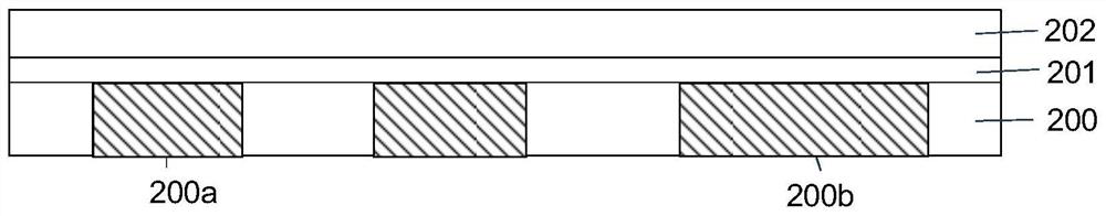
[0035] As introduced in the background art, the exposure of the CMOS metal connection layer in the manufacturing method of the MRAM in the prior art affects device performance and yield. The inventors of the present invention conducted research on the above problems, and proposed a method for preparing a magnetoresistive random access memory, including the following steps: S1, forming an MTJ metal interconnection layer 200a and a CMOS metal connection layer 200b on a CMOS; S2, forming Form the first conductive layer 203a on the MTJ metal interconnection layer 200a, and form the second conductive layer 203b on the CMOS metal connection layer 200b; S3, form the first metal isolation layer 204a on the first conductive layer 203a, and form the second conductive layer 203b on the second conductive layer A second metal isolation layer 204b is formed on the layer 203b, the first metal isolation layer 204a and the second metal isolation layer 204b both include a diffusion barrier layer...

Embodiment 1

[0060] The preparation method of the magnetoresistive random access memory adopted in this embodiment comprises the following steps:

[0061] Forming the MTJ metal interconnection layer 200a and the CMOS metal connection layer 200b on the CMOS by using metal Cu;

[0062] Use SiN or SiCN to form the first etch barrier layer 201 on the first surface of the MTJ metal interconnection layer 200a and the CMOS metal connection layer 200b where the surface away from the CMOS is located, and use SiO 2 A first insulating layer 202 is formed on the first etch stop layer 201, such as figure 1 shown;

[0063] Form a first via hole and a second via hole in the first etching barrier layer 201 and the first insulating layer 202, the first via hole communicates with the MTJ metal interconnection layer 200a, and the second via hole communicates with the MTJ metal interconnection layer 200a Connected, fill metal Cu in the first through hole and the second through hole, form the first conductiv...


PUM

PropertyMeasurementUnit
thicknessaaaaaaaaaa
thicknessaaaaaaaaaa
thicknessaaaaaaaaaa

Abstract

The invention provides a magnetoresistive random access memory and a preparation method thereof. The patent of the present invention proposes to adopt a new type of etching step in the preparation process of magnetoresistive random access memory, including forming a first metal isolation layer on the surface of the first conductive layer connected with the MTJ metal interconnection layer, and forming a first metal isolation layer on the surface of the CMOS A second metal isolation layer is formed on the surface of the second conductive layer connected by the metal connection layer, and both the first metal isolation layer and the second metal isolation layer include a diffusion barrier layer, thereby preventing the etching site from The exposure of the CMOS metal connection layer during the line through hole effectively solves the problem of redeposition of copper and other metal materials on the side walls and channels of the through hole and the formation of various compounds on the metal surface of the through hole during the etching process, and improves the reliability of the device. Yield, reliability, and other performance.

Description

technical field [0001] The invention relates to the field of memory, in particular to a magnetoresistive random access memory and a preparation method thereof. Background technique [0002] Magneto-resistive random access memory (MRAM) is a non-volatile memory whose core is a magnetic tunnel junction (MTJ). Each magnetic tunnel junction is composed of a ferromagnetic free layer and a pinned layer and a non-magnetic layer separating the free layer and the pinned layer. The magnetization direction of the free layer can be reversed by an external magnetic field or current, while the magnetization direction of the pinned layer remains unchanged, and the resistance of the magnetic tunnel junction is related to the relative magnetization direction of the free layer and the fixed layer, when the magnetization direction of the free layer is parallel (antiparallel) to the magnetization direction of the fixed layer, the magnetic tunnel junction exhibits low resistance (high resistanc...

Claims


Application Information

Patent Timeline
Patent Type & Authority Patents(China)
IPC IPC(8): H01L27/22H01L43/08H01L43/12
CPCH10B61/22H10N50/10H10N50/01
Inventor 刘瑞盛杨成成
Owner CETHIK GRP