Method for rapidly determining thickness unevenness reasons of diamond cutting silicon wafers

A technology for diamond cutting and determining methods, which is applied in the field of rapid determination of the reasons for the uneven thickness of diamond-cut silicon wafers, which can solve the problems that cannot be determined quickly and the thickness of silicon wafers is uneven, and achieve the effects of improving abnormal processing efficiency and production efficiency

Active Publication Date: 2019-04-05
KONCA SOLAR CELL
View PDF19 Cites 0 Cited by
  • Summary
  • Abstract
  • Description
  • Claims
  • Application Information

AI Technical Summary

Problems solved by technology

[0004] The purpose of the present invention is to provide a method for quickly determining the cause of the uneven thickness of the diamond-cut silicon wafer to solve the problem in the prior art that the cause cannot be quickly determined when the thickness of the silicon wafer is uneven

Method used


Image

  • Method for rapidly determining thickness unevenness reasons of diamond cutting silicon wafers

Examples


Embodiment Construction

[0015] The technical solution of the present invention will be further described below in conjunction with the accompanying drawings and through specific implementation methods.

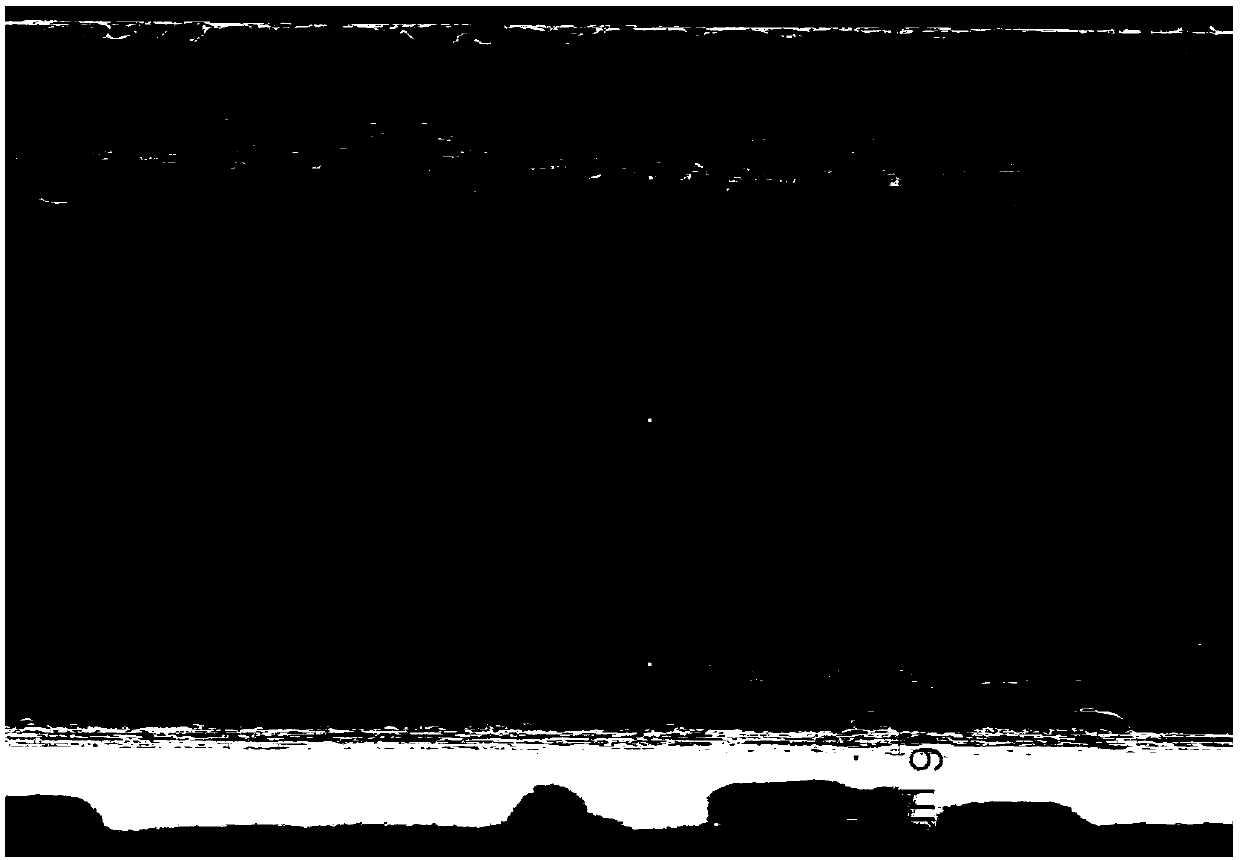
[0016] see figure 1 as shown, figure 1 It is a silicon wafer electron microscope end view of the method for quickly determining the cause of the uneven thickness of the diamond-cut silicon wafer provided by the specific embodiment of the present invention.

[0017] In this embodiment, a method for quickly determining the cause of uneven thickness of a diamond-cut silicon wafer comprises the following steps:

[0018] Step 1: Randomly select a single silicon wafer from the whole silicon wafer as an analysis sample;

[0019] Step 2: vertically fix the end face of the analytical sample preparation on the fixture;

[0020] Step 3: Observe the slice thickness and the original surface morphology area of ​​the end face through an electron microscope, and measure the slice thickness as H = 176.6 microns, t...


PUM


Abstract

The invention discloses a method for rapidly determining thickness unevenness reasons of diamond cutting silicon wafers. The method comprises the following steps of: 1) randomly selecting a single silicon wafer from silicon wafers cut by a whole knife as an analysis sample; 2) vertically fixing an analysis sample preparation end surface on a clamp; and 3) observing a thickness and an original surface morphology area of the end surface through an electron microscope, measuring the thickness as H and the thickness of the original surface morphology area as h1, and if H is greater than h1, determining that silicon wafer thickness unevenness is caused by the position moving of a zero position. The method for rapidly determining thickness unevenness reasons of diamond cutting silicon wafers iscapable of rapidly analyzing and determining the reasons of silicon wafer thickness unevenness and improving the abnormal processing efficiency and is beneficial for improving the production efficiency to a certain extent.

Description

technical field [0001] The invention belongs to the cutting technology of solar silicon wafers, in particular to a method for rapidly determining the cause of uneven thickness of diamond-cut silicon wafers. Background technique [0002] The multi-wire cutting machine uses diamond wire to achieve high-speed cutting, and the cutting feed speed can be increased to 2 times the original, and it uses water to participate in cutting and a small amount of water-based cutting fluid, which can be recycled and reused, environmentally friendly and low energy consumption, greatly improving Cutting costs are reduced, and efficient and environmentally friendly production is truly realized. However, the diamond wire cutting process often causes abnormal problems such as uneven thickness of silicon wafers, and customers often complain about uneven thickness of silicon wafers. [0003] The reason for the uneven thickness of cut silicon wafers may be that there is an inclination angle between...

Claims


Application Information

Patent Timeline
IPC IPC(8): G01N21/88B28D5/00
CPCB28D5/0058G01N21/8851G01N2021/8854G01N2021/8887
Inventor 张爱平何晋康
Owner KONCA SOLAR CELL
Why Eureka
Try Eureka