
Touch display device

A technology for a touch display device and a touch layer is applied in the fields of instruments, electrical digital data processing, computer parts, etc., and can solve the problems of increasing the manufacturing process and cost, unfavorable to the development of thin and light display devices, and increasing the thickness of the display device, etc. Achieve the effect of reducing production processes, improving user experience, and improving accuracy

Active Publication Date: 2019-04-05
WUHAN CHINA STAR OPTOELECTRONICS TECH CO LTD
View PDF7 Cites 8 Cited by
  • Summary
  • Abstract
  • Description
  • Claims
  • Application Information

AI Technical Summary

Problems solved by technology

[0004] The present invention provides a touch display device to solve the problem of the existing touch display device. Since the fingerprint identification module is separately installed, the manufacturing process and cost will be increased, and the thickness of the display device will also increase, which is not conducive to the thinner and lighter display device. technical issues of development

Method used


Image

  • Touch display device
  • Touch display device
  • Touch display device

Examples


Embodiment 1

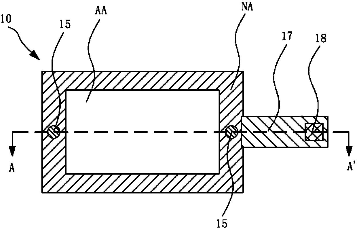
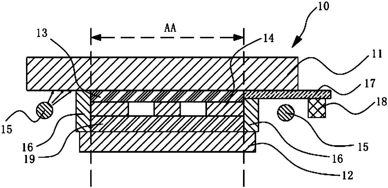
[0038] Please refer to figure 1 with figure 2 , figure 1 It is a top view of this embodiment, figure 2 for figure 1 The schematic cross-sectional view at AA' in the center, this implementation provides a touch display device 10, the touch display device 10 is defined with a display area AA and a non-display area NA, and the non-display area NA surrounds the display area AA set up.

[0039] The touch display device 10 includes a protective layer 11 , a display module 12 , a touch layer 13 , a fingerprint sensor layer 14 , a backlight source 15 , a light shielding layer 16 , and a first adhesive layer 19 .

[0040] Wherein, the protective layer 11 is a light-transmitting substrate, such as a glass substrate, and the protective layer 11 has a first surface and a second surface opposite to each other, and the second surface is used for fingerprint contact of human fingers.

[0041] The touch layer 13 is arranged between the protective layer 11 and the display module 12, the...

Embodiment 2

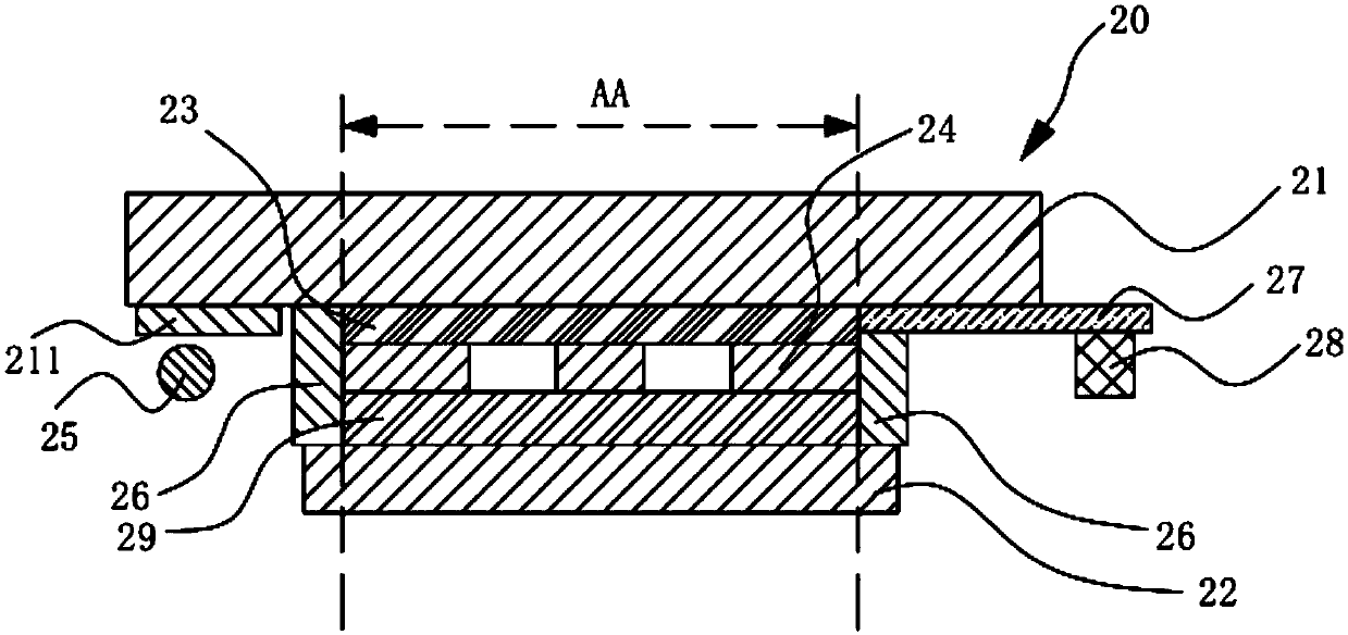
[0051] Such as image 3 As shown, this embodiment provides a touch display device 20, including a protective layer 21, a display module 22, a touch layer 23, a fingerprint sensor layer 24, a backlight 25, a light shielding layer 26, a flexible circuit board 27, and a driver chip 28, and the first adhesive layer 29.

[0052] The above-mentioned structure is the same as or similar to that of the first embodiment, and reference may be made to the description of the related structure of the first embodiment, which will not be repeated here.

[0053] Different from Embodiment 1, the touch display device 20 of this embodiment further includes an optical anti-reflection layer 211, and the optical anti-reflection layer 211 is disposed on the first surface of the protective layer 21 corresponding to the backlight source 25 For the part, the light-enhancing layer is conducive to light transmission, so that the light emitted by the backlight is more used for fingerprint image collection...

Embodiment 3

[0055] Such as Figure 4 As shown, this embodiment provides a touch display device 30, including a protective layer 31, a display module 32, a touch layer 33, a fingerprint sensor layer 34, a backlight 35, a light shielding layer 36, a flexible circuit board 37, and a driver chip 38, and the first adhesive layer 39.

[0056] The above-mentioned structure is the same as or similar to that of the first embodiment, and reference may be made to the description of the related structure of the first embodiment, which will not be repeated here.

[0057] Different from Embodiment 1, the touch display device 30 of this embodiment further includes a light-gathering layer 351, and the light-gathering layer 351 is arranged on the side of the backlight 35 close to the protective layer 31, and can The surface of the backlight 35 is provided with glue or glue with a large refractive index and a high transmittance, so that more light emitted by the light source can be used for fingerprint im...


PUM


Abstract

The invention discloses a touch display device. Including protective layer, Display module, a touch layer and a fingerprint sensor layer, a backlight source; and a light shielding layer, wherein the fingerprint sensor layer and the touch control laminated layer are arranged in a display area of the display device; The fingerprint sensor layer and the touch layer are integrated together, so that afingerprint recognition function can be realized while touch display is realized, production procedures are reduced, the production cost is reduced, the fingerprint recognition precision is improved,and the overall thickness of the display device is reduced.

Description

technical field [0001] The invention relates to the field of display technology, in particular to a touch display device with a high-performance fingerprint identification function. Background technique [0002] At present, mobile electronic devices have developed a method of identifying personal fingerprints for identity authentication, which improves the security of mobile devices. Fingerprint imaging recognition technology is to collect the fingerprint image of the human body through the fingerprint sensor, and then compare it with the existing fingerprint imaging information in the system to judge whether the fingerprint information matches, and then realize the technology of identity recognition. Fingerprint identification technology can be implemented in various ways such as optical imaging, capacitive imaging, and ultrasonic imaging. Relatively speaking, optical fingerprint imaging technology has a relatively good imaging effect and relatively low equipment cost. [...

Claims


Application Information

Patent Timeline
Patent Type & Authority Applications(China)
IPC IPC(8): G06F3/041G06K9/00G02F1/1333
CPCG02F1/13338G06F3/0412G06V40/1318
Inventor 步欢欢
Owner WUHAN CHINA STAR OPTOELECTRONICS TECH CO LTD
Learn More