Eureka AIR delivers breakthrough ideas for toughest innovation challenges, trusted by R&D personnel around the world.

Method and substrate for selective transfer of semiconductor devices

A semiconductor and selective technology, applied in the direction of semiconductor devices, electrical components, circuits, etc., can solve the problems of high implementation cost and high implementation difficulty of LED chips, and achieve the effect of reducing implementation cost and implementation difficulty

Pending Publication Date: 2019-04-05
HC SEMITEK ZHEJIANG CO LTD
View PDF6 Cites 0 Cited by
  • Summary
  • Abstract
  • Description
  • Claims
  • Application Information

AI Technical Summary

Problems solved by technology

[0006] Embodiments of the present invention provide a method and a substrate for selectively transferring semiconductor devices, which can solve the problem of high cost and difficulty in implementing selective transfer of LED chips for different applications of LED chips on self-luminous display screens in the prior art question

Method used


Image

  • Method and substrate for selective transfer of semiconductor devices
  • Method and substrate for selective transfer of semiconductor devices
  • Method and substrate for selective transfer of semiconductor devices

Examples


Embodiment Construction

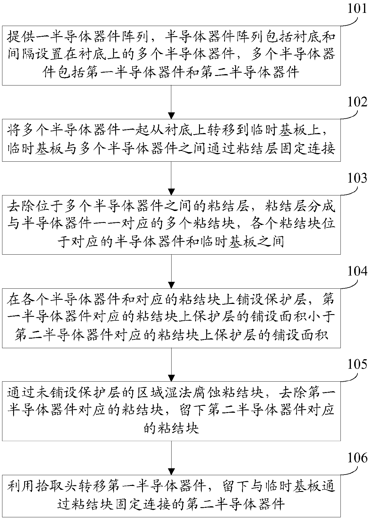
[0048] In order to make the object, technical solution and advantages of the present invention clearer, the implementation manner of the present invention will be further described in detail below in conjunction with the accompanying drawings.

[0049] An embodiment of the present invention provides a method for selectively transferring a semiconductor device. figure 1 It is a flow chart of a method for selectively transferring a semiconductor device provided by an embodiment of the present invention. see figure 1 , the method includes:

[0050] Step 101: Provide a semiconductor device array, the semiconductor device array includes a substrate and a plurality of semiconductor devices arranged on the substrate at intervals, the plurality of semiconductor devices include a first semiconductor device and a second semiconductor device.

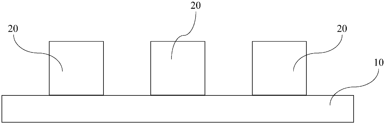
[0051] figure 2 A schematic structural diagram of a semiconductor device array provided by an embodiment of the present invention. Wherein, 10...


PUM


Abstract

The invention discloses a method and substrate for selective transfer of semiconductor devices, and belongs to the technical field of semiconductors. The method includes steps: providing a semiconductor device array, wherein the semiconductor device array comprises a plurality of semiconductor devices, and the plurality of semiconductor devices comprise first semiconductor devices and second semiconductor devices; transferring the plurality of semiconductor devices on a temporary substrate, wherein the temporary substrate is fixedly connected with the plurality of semiconductor devices througha bonding layer; removing the bonding layer between the plurality of semiconductor devices, wherein the bonding layer is divided into a plurality of bonding blocks; laying protective layers on the semiconductor devices and the corresponding bonding blocks, wherein the laying area of the protective layers on the bonding blocks corresponding to the first semiconductor devices is smaller than the laying area of the protective layers on the bonding blocks corresponding to the second semiconductor devices; eroding the bonding blocks by employing a wet method through the area without laying the protective layer; and transferring the first semiconductor devices by employing a pickup head, and remaining the second semiconductor devices. According to the method and substrate, the cost and the realization difficulty are greatly reduced.

Description

technical field [0001] The invention relates to the technical field of semiconductors, in particular to a method and a substrate for selectively transferring semiconductor devices. Background technique [0002] Light Emitting Diode (English: Light Emitting Diode, referred to as: LED) is a semiconductor diode that can convert electrical energy into light energy. Chips are the core components of LEDs and are widely used in self-luminous displays. With the continuous improvement of display quality and display requirements of self-luminous display screens, the display area and display density of self-luminous display screens continue to increase, and the number of LED chips used on self-luminous display screens also continues to increase. [0003] When applying LED chips on self-luminous display screens, it is necessary to transfer a large number of LED chips to the backplane. At present, a pick-up head is usually used to grab a large number of LED chips at one time and place ...

Claims


Application Information

Patent Timeline
Patent Type & Authority Applications(China)
IPC IPC(8): H01L33/00H01L33/44H01L33/48
CPCH01L33/44H01L33/483H01L2933/0033H01L33/0093
Inventor 陈亮马非凡王江波
Owner HC SEMITEK ZHEJIANG CO LTD
Why Eureka
Eureka Blog
Learn More