A circuit board level product radiation emission electromagnetic compatibility simulation method

An electromagnetic compatibility and radiation emission technology, applied in CAD circuit design, electrical digital data processing, special data processing applications, etc., can solve complex problems and achieve simple results

Pending Publication Date: 2019-04-09
BEIJING INST OF REMOTE SENSING EQUIP
View PDF2 Cites 3 Cited by
  • Summary
  • Abstract
  • Description
  • Claims
  • Application Information

AI Technical Summary

Problems solved by technology

The internal electromagnetic compatibility of the product directly affects the product performance, and the electromagnetic compatibility of the circuit board level product directly affects the final state of the product. Simulation of it can predict potential risks in advance and prevent problems before they happen. Electromagnetic Interference Problems of Radiation Emission Projects of High-level Products

Method used


Image

  • A circuit board level product radiation emission electromagnetic compatibility simulation method

Examples


Embodiment Construction

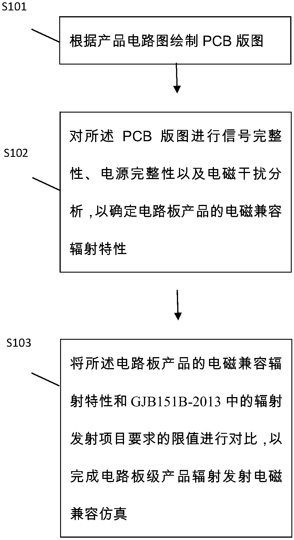
[0011] The present invention will be described in further detail below in conjunction with the accompanying drawings and specific embodiments. According to the following description and claims, the advantages and features of the present invention will be more clear. It should be noted that all the drawings are in very simplified form and inaccurate scales, and are only used to facilitate and clearly assist the purpose of illustrating the embodiments of the present invention.

[0012] It should be noted that, in order to clearly illustrate the content of the present invention, the present invention specifically cites multiple embodiments to further explain different implementation modes of the present invention, wherein the multiple embodiments are enumerated rather than exhaustive. In addition, for the sake of brevity of description, the content mentioned in the previous embodiment is often omitted in the latter embodiment, therefore, the content not mentioned in the later embo...


PUM


Abstract

The invention discloses a circuit board level product radiation emission electromagnetic compatibility simulation method. The method comprises the steps: drawing a PCB layout according to a product circuit diagram; Analyzing the signal integrity, the power supply integrity and the electromagnetic interference of the PCB layout to determine the electromagnetic compatibility radiation characteristics of the circuit board product; And comparing the electromagnetic compatibility radiation characteristic of the circuit board product with a limit value required by a radiation emission project in GJB151B to complete the radiation emission electromagnetic compatibility simulation of the circuit board product. Through the steps of PCB layout introduction, PCB lamination parameter modification, excitation source addition, simulation setting, result post-processing and the like, the electromagnetic compatibility radiation characteristic of a circuit board product is determined, and the electromagnetic compatibility radiation characteristic of the circuit board product are determined and compared with The limits required by the radiation emission items in the national military standard GJB151B-2013. The method can effectively realize the emission level of electromagnetic radiation of products through the national military standard GJB151B-2013 certification, and provide an important theoretical basis for the subsequent product optimization design..

Description

technical field [0001] The invention discloses a radiation emission electromagnetic compatibility simulation method, in particular to a circuit board-level product radiation emission electromagnetic compatibility simulation method. Background technique [0002] Equipment-level products are composed of circuit board-level products, and the electromagnetic radiation of circuit board-level products can reflect the internal electromagnetic compatibility performance of the product. The PCB board is the coupling channel for the electromagnetic interference of the product, and the quality of the PCB board will affect the quality of EMI source suppression. The internal electromagnetic compatibility of the product directly affects the product performance, and the electromagnetic compatibility of the circuit board level product directly affects the final state of the product. Simulation of it can predict potential risks in advance and prevent problems before they happen. Electromagne...

Claims


Application Information

Patent Timeline
Patent Type & Authority Applications(China)
IPC IPC(8): G06F17/50
CPCG06F30/392G06F30/39
Inventor 刘哲
Owner BEIJING INST OF REMOTE SENSING EQUIP
Why Eureka
Try Eureka