OLED substrate and manufacturing method thereof, OLED display device

A substrate and bottom plate technology, used in semiconductor/solid-state device manufacturing, semiconductor devices, electrical components, etc., can solve problems such as poor, open circuit conduction uniformity, fracture, etc.

Active Publication Date: 2021-03-26
BOE TECH GRP CO LTD
View PDF5 Cites 0 Cited by
  • Summary
  • Abstract
  • Description
  • Claims
  • Application Information

AI Technical Summary

Problems solved by technology

[0004] Embodiments of the present invention provide an OLED substrate and its preparation method, and an OLED display device, which can solve the problem of open circuit or conductive uniformity caused by the breakage of the second electrode layer at the junction between the side of the pixel defining layer located in the opening area and the first surface bad question

Method used


Image

  • OLED substrate and manufacturing method thereof, OLED display device
  • OLED substrate and manufacturing method thereof, OLED display device
  • OLED substrate and manufacturing method thereof, OLED display device

Examples


Embodiment Construction

[0034] The following will clearly and completely describe the technical solutions in the embodiments of the present invention with reference to the accompanying drawings in the embodiments of the present invention. Obviously, the described embodiments are only some, not all, embodiments of the present invention. Based on the embodiments of the present invention, all other embodiments obtained by persons of ordinary skill in the art without making creative efforts belong to the protection scope of the present invention.

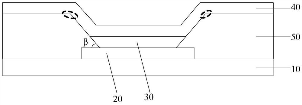
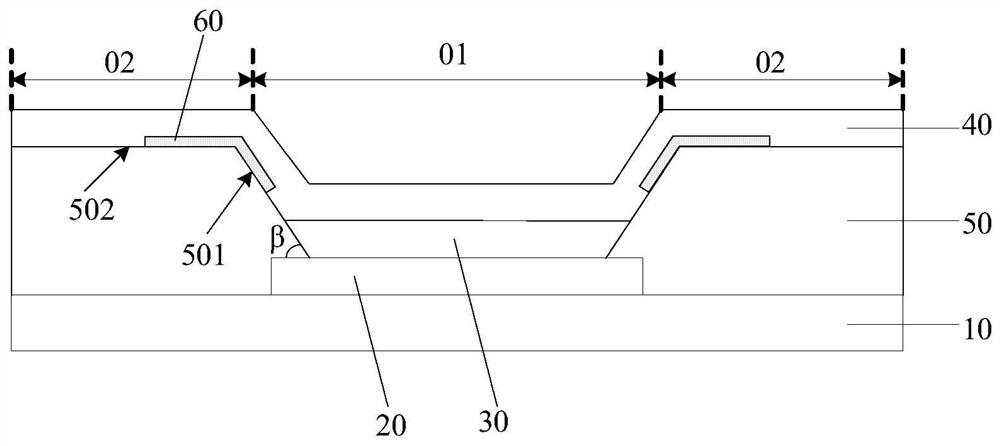
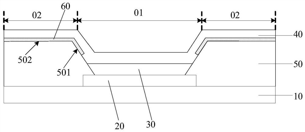
[0035] In related technologies, the OLED substrate includes a plurality of sub-pixels, and adjacent sub-pixels are separated by a Pixel Definition Layer (PDL for short, also called a bank), for example figure 1 As shown, each sub-pixel includes a first electrode 20 , a light emitting layer 30 and a second electrode sequentially disposed on the bottom plate 10 . Each opening area of ​​the pixel defining layer 50 exposes a first electrode 20 , the light emitting...


PUM

PropertyMeasurementUnit
widthaaaaaaaaaa
widthaaaaaaaaaa
widthaaaaaaaaaa

Abstract

Embodiments of the present invention provide an OLED substrate and its preparation method, and an OLED display device, which relate to the field of display technology and can solve the problem of disconnection caused by the breakage of the second electrode layer at the junction between the side of the pixel defining layer located in the opening area and the first surface Or the problem of poor conductivity uniformity. The OLED substrate includes: a plurality of first electrodes arranged on the bottom plate; a pixel defining layer including a plurality of opening regions, each of which exposes one of the first electrodes; a light emitting layer arranged in the opening regions a second electrode layer disposed on the light-emitting layer and covering the pixel defining layer; an auxiliary electrode extending from the side of the pixel defining layer located in the opening region to the first surface, and connected to the pixel defining layer The second electrode layer is in contact; the first surface is the surface of the pixel defining layer away from the bottom plate.

Description

technical field [0001] The invention relates to the field of display technology, in particular to an OLED substrate, a preparation method thereof, and an OLED display device. Background technique [0002] OLED (Organic Light Emitting Diode, Organic Light Emitting Diode) display device has a series of advantages such as self-luminescence, fast response speed, high brightness, full viewing angle, and flexible display, so it has become a highly competitive and promising next-generation display device. A generation of display devices. [0003] An OLED display device includes an anode, a cathode, and a light-emitting layer. When a voltage is applied to the anode and the cathode, the light-emitting layer will emit light. At present, OLED display devices realize full-color display in two ways, one is that the light-emitting layer emits white light, and the three primary colors are obtained by setting a color film layer (Color Film, CF for short). The other is that the light-emitt...

Claims


Application Information

Patent Timeline
Patent Type & Authority Patents(China)
IPC IPC(8): H01L27/32H01L51/52H01L51/56
CPCH10K59/122H10K59/131H10K50/814H10K50/824H10K59/1201H10K71/00
Inventor 宋莹莹
Owner BOE TECH GRP CO LTD
Why Eureka
Try Eureka