

Camera module and mobile terminal
A camera module and photosensitive chip technology, which is applied in the field of photography, can solve the problems of restricting mobile terminals, and achieve the effects of reducing power consumption, height, and size
- Summary
- Abstract
- Description
- Claims
- Application Information
AI Technical Summary
Problems solved by technology
Method used
Image

Examples
Embodiment Construction
[0021] In order to enable those skilled in the art to better understand the technical solutions in the present application, the technical solutions in the embodiments of the present application will be clearly and completely described below in conjunction with the drawings in the embodiments of the present application. Obviously, the described The embodiments are only some of the embodiments of the present application, but not all of them. Based on the embodiments in this application, all other embodiments obtained by persons of ordinary skill in the art without creative efforts shall fall within the scope of protection of this application.
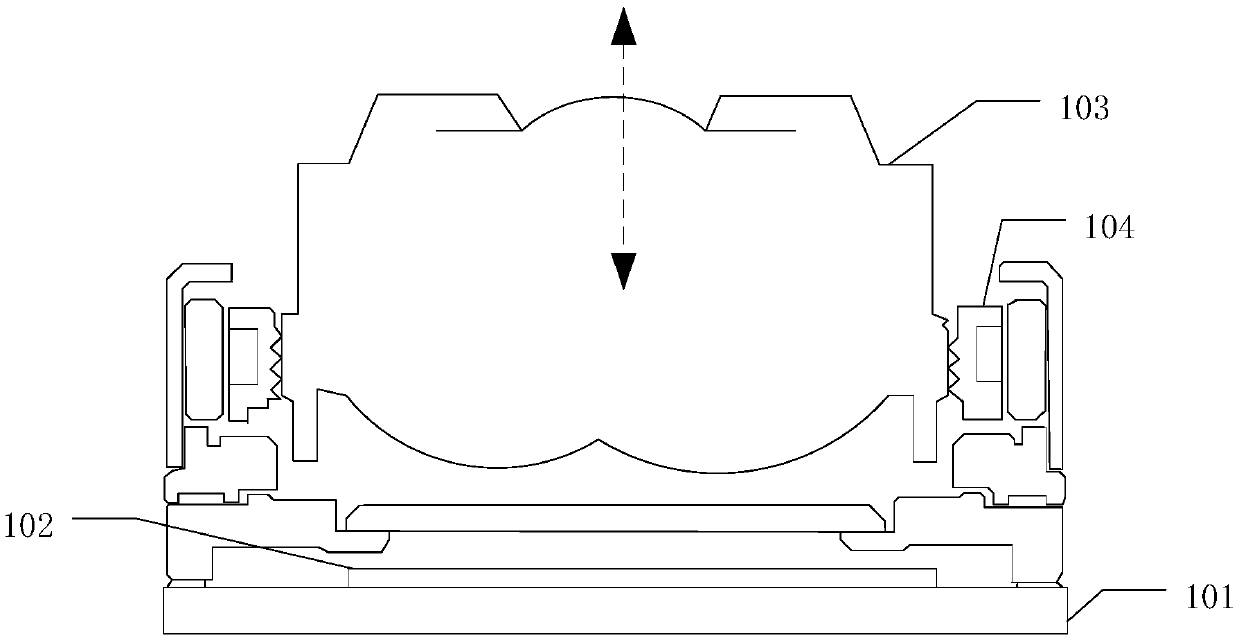
[0022] figure 1 shows a schematic structural diagram of a camera module in a mobile terminal in the related art, from figure 1 As can be seen in the figure, the camera module includes a circuit board 101 , a photosensitive chip 102 , a lens 103 and a focus motor 104 . When focusing, the focus motor 104 controls the lens 103 along the op...
PUM
 Abstract
Description
Claims
Application Information