Optical bistable device applied to all-optical switch and optical memory

A bistable device, all-optical switch technology, applied in the field of all-optical communication systems, to achieve the effect of enhancing third-order nonlinear effects and reducing thresholds

Active Publication Date: 2019-04-16
HUBEI UNIV OF SCI & TECH
View PDF5 Cites 7 Cited by
  • Summary
  • Abstract
  • Description
  • Claims
  • Application Information

AI Technical Summary

Problems solved by technology

And SPPs can only be excited in meta

Method used


Image

  • Optical bistable device applied to all-optical switch and optical memory
  • Optical bistable device applied to all-optical switch and optical memory
  • Optical bistable device applied to all-optical switch and optical memory

Examples


Embodiment Construction

[0038] The following are specific embodiments of the present invention and in conjunction with the accompanying drawings, the technical solutions of the present invention are further described, but the present invention is not limited to these embodiments.

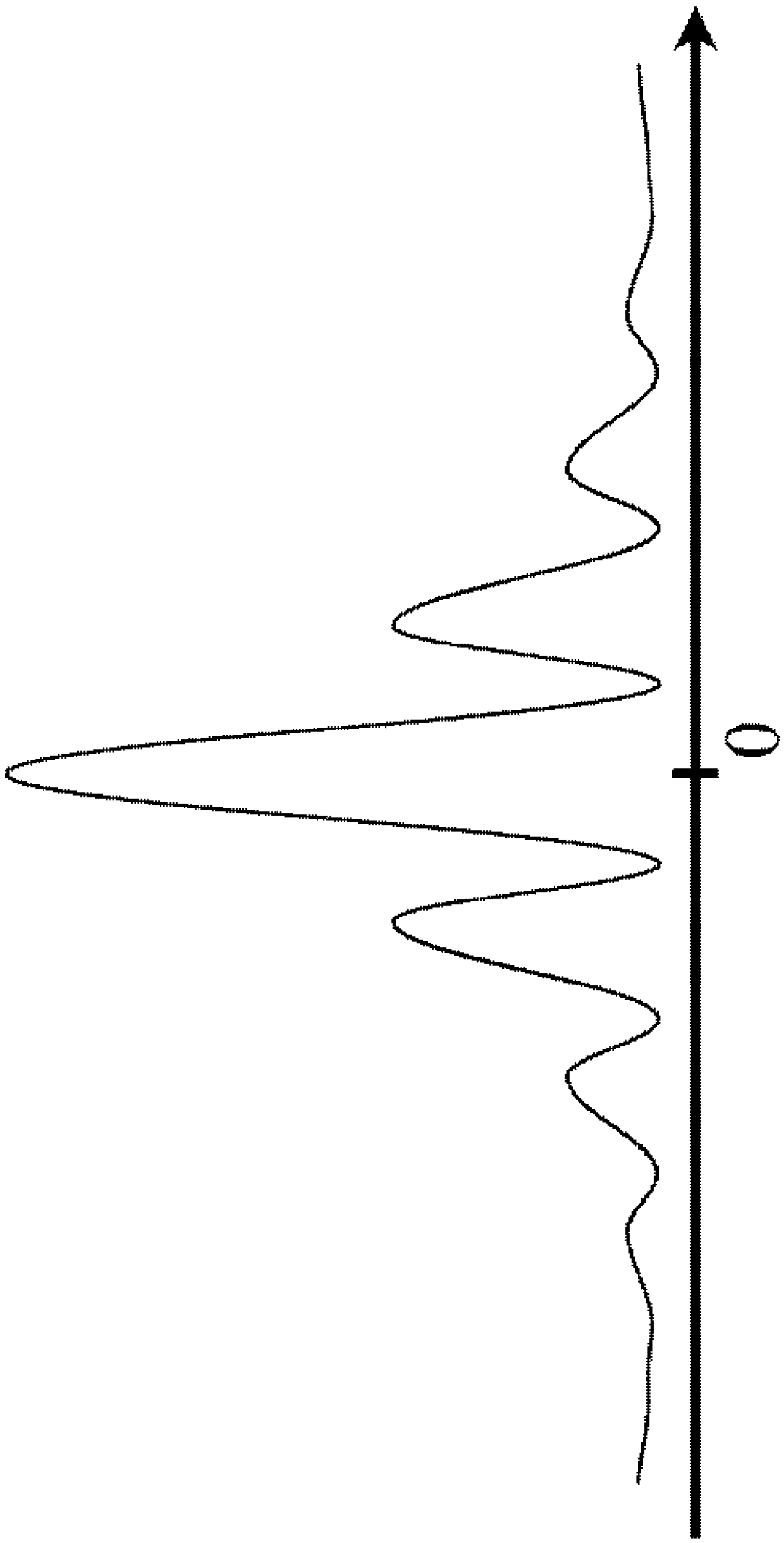
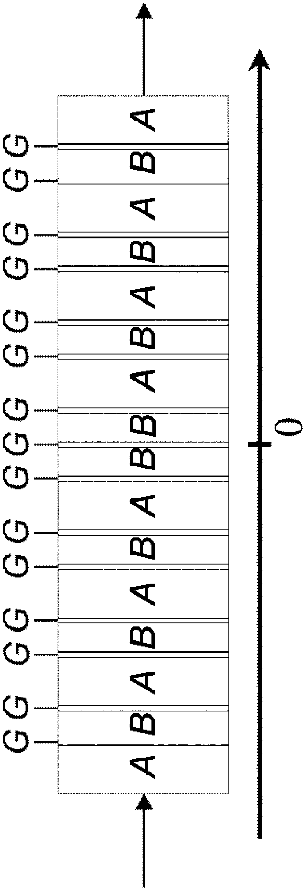
[0039] Such as figure 1As shown, the optical bistable device is a multilayer structure composed of eight dielectric layers A, eight dielectric layers B and fifteen graphene layers G, and the optical bistable device is from the upper surface to the lower surface Dielectric layer one A, graphene layer G, dielectric layer two B, graphene layer G, dielectric layer one A, graphene layer G, dielectric layer two B, dielectric layer one A, graphene layer G, dielectric layer two B. Dielectric layer one A, graphene layer G, dielectric layer two B, graphene layer G, dielectric layer two B, graphene layer G, dielectric layer one A, graphene layer G, dielectric layer two B, graphene layer G, dielectric layer one A, graphene layer G, d...


PUM

PropertyMeasurementUnit
Thicknessaaaaaaaaaa
Thicknessaaaaaaaaaa

Abstract

The invention provides an optical bistable device applied to an all-optical switch and an optical memory, which belongs to the technical field of all-optical communication systems. The optical bistable device has a multilayer structure formed by eight first dielectric layers, eight second dielectric layers and fifteen graphene layers, specifically from the upper surface to the lower surface in sequence, a first dielectric layer, a graphene layer, a second dielectric layer, a graphene layer, a first dielectric layer, a graphene layer, a second dielectric layer, a first dielectric layer, a graphene layer, a second dielectric layer, a first dielectric layer, a graphene layer, a second dielectric layer, a graphene layer, a second dielectric layer, a graphene layer, a first dielectric layer, agraphene layer, a second dielectric layer, a graphene layer, a first dielectric layer, a graphene layer, a second dielectric layer, a graphene layer, a first dielectric layer, a graphene layer, a second dielectric layer, a graphene layer and a first dielectric layer. The optical bistable device applied to the all-optical switch and the optical memory has the advantages of reducing the optical bistable threshold.

Description

technical field [0001] The invention belongs to the technical field of all-optical communication systems, and relates to an optical bistable device applied to all-optical switches and optical memories. Background technique [0002] With the development of all-optical network and information detection technology, there is an urgent need to develop all-optical switches and optical memories. The material-based optical bistability effect can realize all-optical switches and optical memories. [0003] In the past, surface plasmon polaritons (SPPs) or Fabry-Perot cavity structures were generally used to enhance the localization of the electric field, and then materials with large nonlinear coefficients were used to achieve low-threshold optical dual steady state. [0004] SPPs require TM waves to be generated in metals or graphene, and SPPs only go along the surface of the material. Moreover, SPPs can only be excited in metamaterials and Kretschmann structures. [0005] As an ...

Claims


Application Information

Patent Timeline
IPC IPC(8): G02F3/02
CPCG02F3/024
Inventor 赵东
Owner HUBEI UNIV OF SCI & TECH
Why Eureka
Try Eureka