Card-making substrate, preparation method thereof and IC card or electronic tag containing card-making substrate

An electronic label, card substrate technology, applied in chemical instruments and methods, cards, manufacturing tools, etc., can solve the problems of greatly reduced apparent brightness of IC cards, poor practical application effects, violations, etc., so as not to damage the appearance effect, Effects of reduced gloss, long read and write distances

Inactive Publication Date: 2019-04-19
TIANJIN BOYUAN NEW MATERIALS
View PDF11 Cites 2 Cited by
  • Summary
  • Abstract
  • Description
  • Claims
  • Application Information

AI Technical Summary

Problems solved by technology

[0004] Another way of thinking is to achieve the purpose of increasing the reading and writing distance of the non-contact card by improving the composition or structure of the card-making material of the non-contact card. For example, a non-contact IC card bonded with a holographic laser film is disclosed in CN107529649A , including an IC card chip and a card structure, the IC card chip is arranged in the card structure, the card structure includes an upper side card and a lower side card structure, and the upper side card structure includes an IC card that is sequentially arranged on the IC chip from the inside to the outside Holographic PET / PVC laser plastic layer group, printing layer, PET / PVC film layer, etc. Holographic PET / PVC laser plastic layer group includes PET / PVC plastic layer, glue layer, combination layer, metal plating Layer / nano new material layer, PET / PVC base film layer, etc., form a holographic laser pattern on the metallized layer / nano new material layer, which is replaced by setting the thickness of the metallized layer / nano new material layer to 150±50 angstroms. Ordinary aluminized films with a thickness of 380±50 angstroms can improve the reading and writing distance of the non-contact IC card to a certain extent, and the improvement rate is about 10-20%, although this method has a certain increase in the non-contact IC card. However, the apparent brightness of the obtained IC card will be greatly reduced, which violates the original intention of applying laser aluminized film to the field of card making to provide personalized modification effects, and the actual application effect is poor.

Method used


Image

  • Card-making substrate, preparation method thereof and IC card or electronic tag containing card-making substrate
  • Card-making substrate, preparation method thereof and IC card or electronic tag containing card-making substrate
  • Card-making substrate, preparation method thereof and IC card or electronic tag containing card-making substrate

Examples


Embodiment 1

[0059] Prepare the laser card substrate 1 through the following steps:

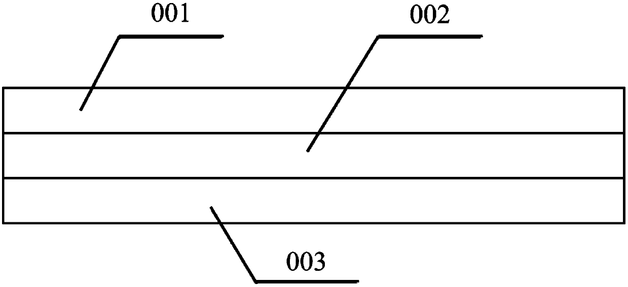
[0060] In step (1), one layer of adhesive glue with a thickness of 30 μm is coated on the side of the aluminum-coated film containing the aluminum film. Substrate layer 003 is laminated and cut to obtain a pretreated substrate;

[0061] Step (2), carry out laser etching process to the surface of the aluminized film layer in the pretreatment substrate obtained in step (1), form continuous scratches on the surface of the aluminum film, the width of the scratches is 0.05mm, and the depth is 55nm, the scratches divide the aluminum film of the aluminized film into 20 non-connected square areas with a side length of 1 mm to obtain the laser card substrate.

[0062] Wherein, the aluminized film described in the step (1) is a PET film coated with an aluminum film on the surface, the thickness of the PET film is 0.08mm, and the thickness of the aluminum film is 35nm.

[0063] The substrate layer 003 described in...

Embodiment 2

[0068] Prepare the laser card substrate 2 through the following steps:

[0069] The only difference from Example 1 is that the scratches divide the aluminum film of the aluminized film into 12 non-connected square areas with a side length of 1.29 mm.

[0070] Scratch makes the aluminum film surface in the aluminized film layer of the laser card substrate 2 that embodiment 2 obtains has such as image 3 pattern shown.

Embodiment 3

[0072] Prepare the laser card substrate 3 through the following steps:

[0073] The only difference from Example 1 is that the scratches divide the aluminum film of the aluminized film into 8 unconnected right-angled triangular areas with side lengths of 2 mm, 2.5 mm and 3.2 mm, respectively.

[0074] Scratch makes the aluminum film surface in the aluminized film layer of the laser card substrate 3 that embodiment 3 obtains has such as Figure 4 pattern shown.


PUM

PropertyMeasurementUnit
widthaaaaaaaaaa
thicknessaaaaaaaaaa
thicknessaaaaaaaaaa

Abstract

The invention provides a card making substrate. The invention relates to a preparation method and an IC card or an electronic tag containing the same. wherein the card making substrate comprises an aluminized film layer, a bonding glue layer and a base material layer which are overlapped in sequence, at least one continuous scratch exists on the surface of the aluminized film layer, the depth of the scratch is greater than the thickness of an aluminum film in the aluminized film layer, and the scratch and the edge of the aluminized film layer divide the aluminum film in the aluminized film layer into at least two areas which are mutually connected; According to the invention, at least one continuous scratch is simply added to the surface of the aluminum-plated film layer in a common card-making substrate; The aluminum film is divided into at least two areas which are not connected with each other, so that the non-contact IC card or electronic tag manufactured by the card manufacturingsubstrate has a longer read-write distance, and meanwhile, the appearance effect of the aluminum-plated film with a laser effect is not damaged.

Description

technical field [0001] The invention belongs to the technical field of IC card making, and in particular relates to a card making substrate, a preparation method thereof and an IC card or an electronic label containing the same. Background technique [0002] In recent years, the new card-making materials with distinct individual characteristics represented by laser card-making substrates have attracted extensive attention from domestic and foreign related companies. Laser card-making substrates are a kind of laser-coated aluminum film and plastic (usually PVC material) sheets are combined together to obtain a card material with a laser appearance effect. This material can be combined with other card making materials through lamination or thermal lamination process, and is used in the manufacture of financial cards, high-end VIP cards and various smart cards. However, the above-mentioned card making materials usually contain a metal layer. When it is applied to non-contact ca...

Claims


Application Information

Patent Timeline
Patent Type & Authority Applications(China)
IPC IPC(8): G06K19/02G06K19/077
CPCG06K19/022G06K19/07722B23K2101/36B23K2103/10B23K2103/172B23K26/359B23K26/60G06K19/02B32B7/12B32B2255/10B32B2270/00B32B2425/00B32B2250/02B32B27/365B32B2255/26B32B2307/732B32B27/36B32B27/302B32B27/304B32B2250/24B32B27/08B23K26/362B32B15/09B32B15/20G06K19/0772
Inventor 刘柏松李维腾飞鹿秀山李春刚
Owner TIANJIN BOYUAN NEW MATERIALS
Why Eureka
Try Eureka