

Device and method for wafer test temperature adjustment
A technology for temperature regulation and wafer testing, which is applied in semiconductor/solid-state device testing/measurement, electrical components, circuits, etc., can solve problems such as uneven temperature distribution of wafers, and achieve the goal of solving uneven temperature distribution and improving accuracy Effect
- Summary
- Abstract
- Description
- Claims
- Application Information
AI Technical Summary
Problems solved by technology
Method used
Image

Examples
Embodiment Construction
[0025] The present invention will be described below in conjunction with the accompanying drawings and specific embodiments.
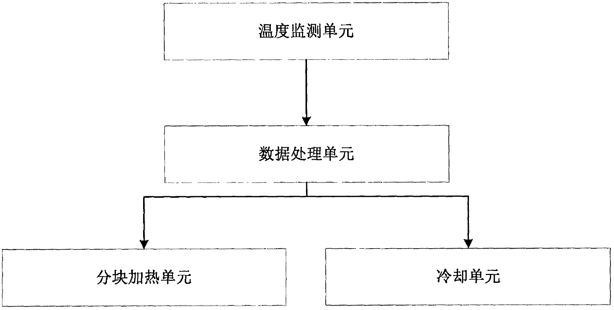
[0026] The invention discloses a device for adjusting the temperature of a wafer test, comprising:
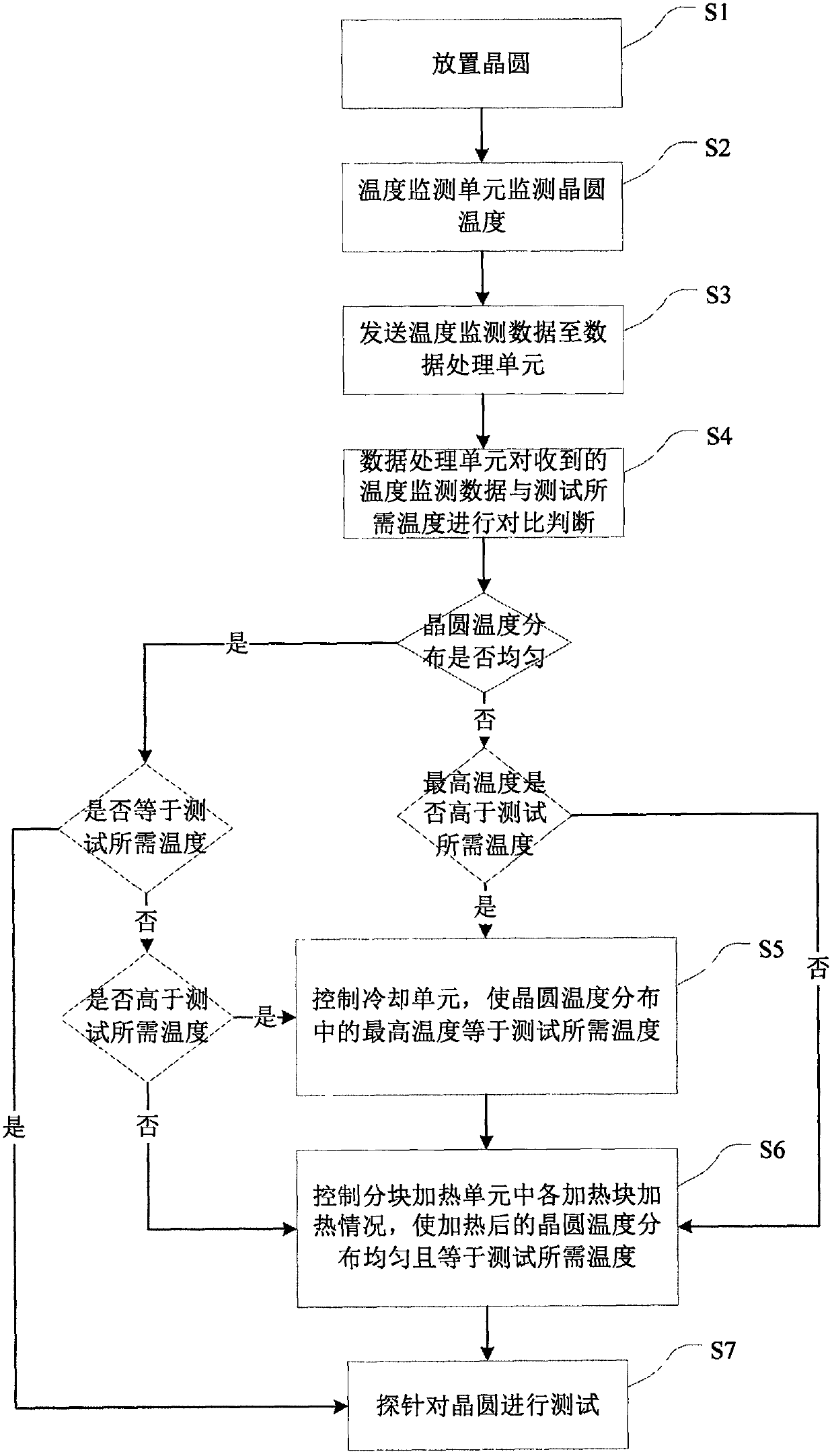
[0027] The temperature monitoring unit is used for real-time temperature monitoring of the wafer, consisting of multiple temperature sensors, and sending the temperature monitoring data to the data processing unit;
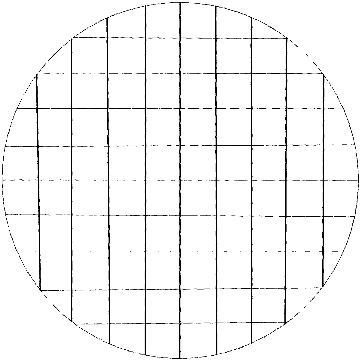
[0028] The block heating unit is used to heat the wafer. It is composed of multiple heating blocks. The number and distribution of the heating blocks and the temperature sensors in the temperature monitoring unit are consistent. The heating conditions of each heating block can be adjusted independently;
[0029] The cooling unit is used to cool the wafer, and consists of a cooling machine, a low-temperature medium supply flow path, a low-temperature medium supply control valve, a low-temperature medium flow path, a low-temperature medium re...
PUM
 Abstract
Description
Claims
Application Information