Display device and manufacturing method thereof

A display device and manufacturing method technology, applied in the direction of final product manufacturing, sustainable manufacturing/processing, semiconductor/solid-state device manufacturing, etc., capable of solving problems such as limited adhesion

Active Publication Date: 2019-04-23
WUHAN CHINA STAR OPTOELECTRONICS SEMICON DISPLAY TECH CO LTD
View PDF9 Cites 11 Cited by
  • Summary
  • Abstract
  • Description
  • Claims
  • Application Information

AI Technical Summary

Problems solved by technology

[0004] However, for a display device with a double-layer organic PI film, due to the limited adhesion between the organic PI film and the inorganic layer, and a neutral axis of the bending area (Bending Area) of the display device is set at The metal axis layer that is prone to bending, therefore, at a start position, a middle position, and an end position of the bending region, the separation due to the organic PI film and the inorganic layer is prone to occur.

Method used


Image

  • Display device and manufacturing method thereof
  • Display device and manufacturing method thereof
  • Display device and manufacturing method thereof

Examples


Embodiment Construction

[0026] The description of the following embodiments refers to the attached drawings to illustrate specific embodiments that the present invention can be implemented. Furthermore, the directional terms mentioned in the present invention, such as up, down, top, bottom, front, back, left, right, inside, outside, side, surrounding, center, horizontal, horizontal, vertical, vertical, axial, The radial direction, the uppermost layer or the lowermost layer, etc., are only the direction of reference to the attached drawings. Therefore, the directional terms used are used to describe and understand the present invention, rather than to limit the present invention.

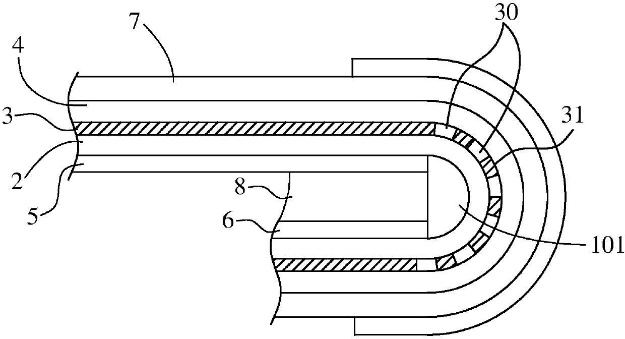
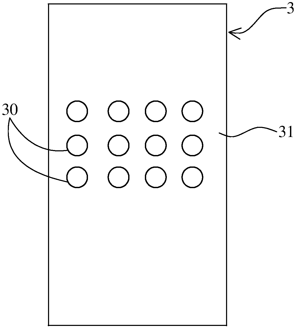
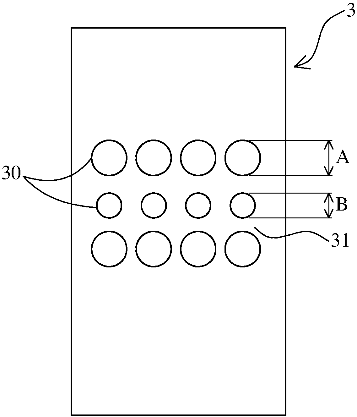
[0027] Please refer to figure 1 Shown is a schematic diagram of a preferred embodiment of the display device of the present invention. The display device includes a first flexible substrate layer 2, a buffer layer 3, a second flexible substrate layer 4, a first backplane 5 and a second backplane 6. The present invention will...


PUM


Abstract

The invention discloses a display device and a manufacturing method thereof. The display device comprises a first flexible substrate layer, at least one buffer layer and a second flexible substrate layer. The second flexible substrate layer is formed on the buffer layer. The buffer layer is formed on the first flexible substrate layer. A patterned pattern is formed in a bending area of the bufferlayer, so that the first flexible substrate layer is attached to the second flexible substrate layer through the pattern.

Description

Technical field [0001] The present invention relates to a display device, in particular to an active matrix organic light emitting diode display device. Background technique [0002] Organic Light Emitting Diode (OLED) display is a self-luminous display. According to the driving mode, it can be divided into passive matrix driving organic light emitting diode (Passive Matrix Driving OLED, PMOLED) displays and active matrix driving organic light emitting diode (Active Matrix Driving OLED, AMOLED) displays. Because AMOLED displays have the advantages of low manufacturing cost, high response speed, power saving, DC drive for portable devices, large operating temperature range, etc., more and more active matrix drive organic light emitting diode displays are applied to various Among the high-performance display fields. [0003] Furthermore, in the display device of AMOLED displays, a first flexible substrate layer, a buffer layer, and a second flexible substrate layer are fabricated o...

Claims


Application Information

Patent Timeline
Patent Type & Authority Applications(China)
IPC IPC(8): H01L27/32H01L51/00H01L21/77
CPCH10K59/127H10K77/111H10K59/1201Y02E10/549Y02P70/50H10K71/00H10K59/1275H10K2102/311
Inventor 向明
Owner WUHAN CHINA STAR OPTOELECTRONICS SEMICON DISPLAY TECH CO LTD
Why Eureka
Try Eureka