Thin film transistor, manufacturing method thereof and display device

A technology of thin film transistors and manufacturing methods, which is applied in the direction of transistors, semiconductor/solid-state device manufacturing, semiconductor devices, etc., and can solve the problems of large plane size, channel width, length and height of thin film transistors, etc.

Active Publication Date: 2019-04-26
BOE TECH GRP CO LTD +1
View PDF3 Cites 6 Cited by
  • Summary
  • Abstract
  • Description
  • Claims
  • Application Information

AI Technical Summary

Problems solved by technology

[0005] The present invention provides a thin film transistor, a manufacturing method thereof, and a display device, which can solve the problem in the related

Method used


Image

  • Thin film transistor, manufacturing method thereof and display device
  • Thin film transistor, manufacturing method thereof and display device
  • Thin film transistor, manufacturing method thereof and display device

Examples


Embodiment Construction

[0096] In order to make the object, technical solution and advantages of the present invention clearer, the implementation manner of the present invention will be further described in detail below in conjunction with the accompanying drawings.

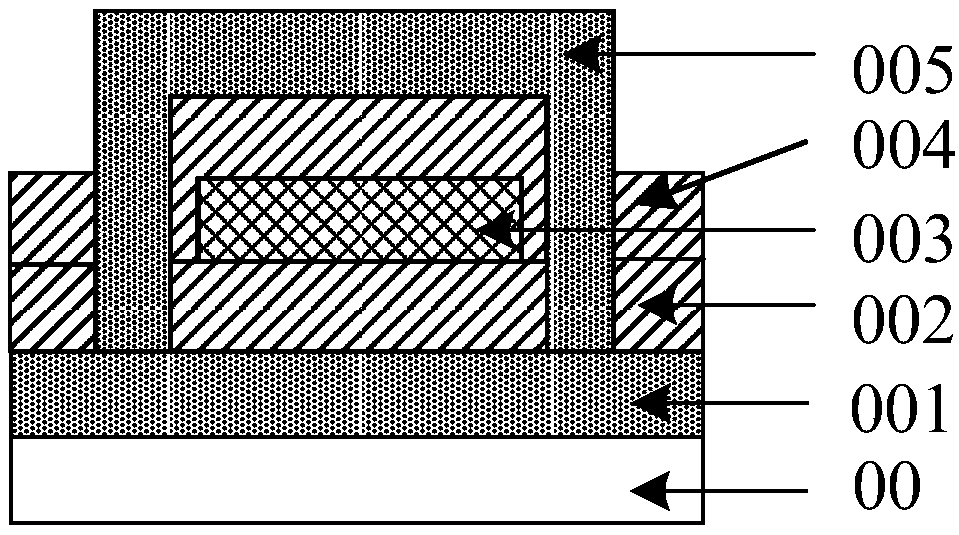
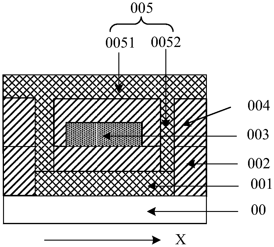
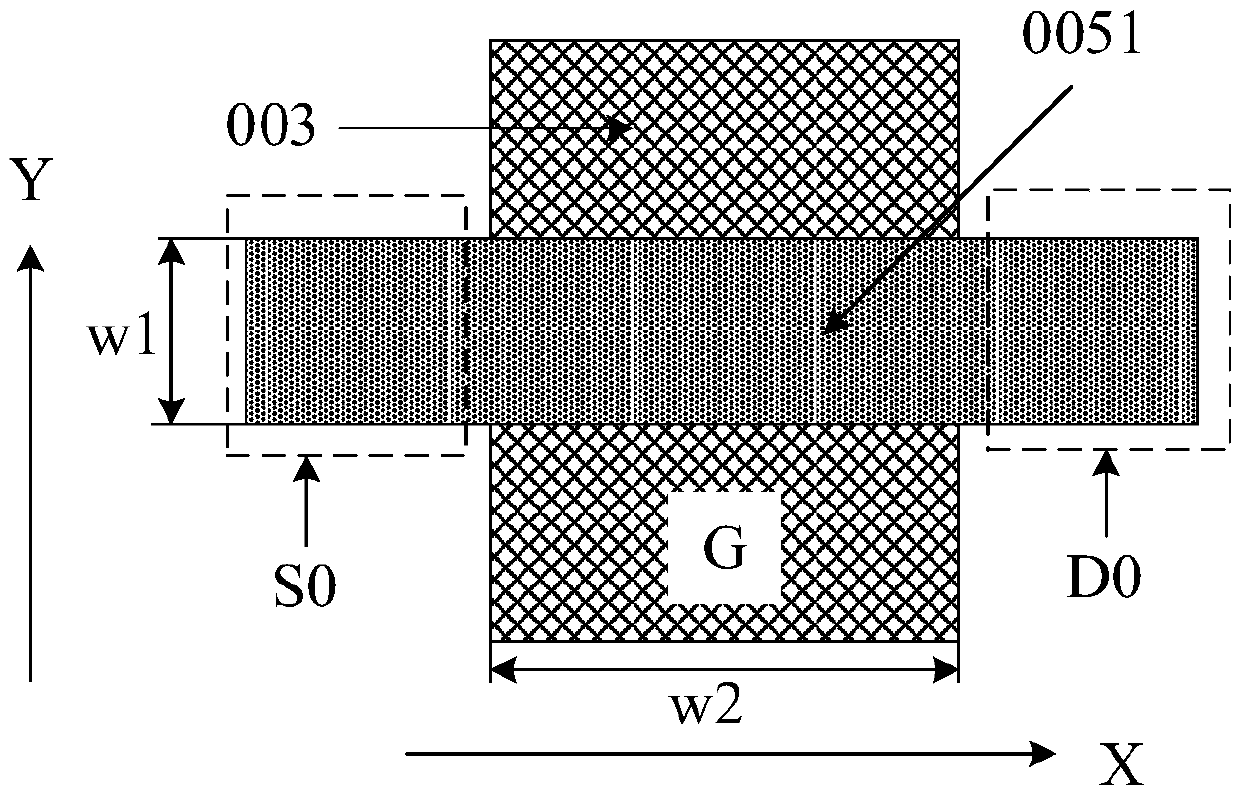
[0097] In a thin film transistor, the part of the active layer overlapping with the gate layer is the channel of the thin film transistor. Wherein, the overlapping of the active layer and the gate layer may refer to the overlapping of the orthographic projections of the two on the base substrate. The active layer and the gate layer are usually in a strip structure, the width direction of the active layer is perpendicular to the width direction of the gate layer, and the width of the active layer is generally smaller than the length of the gate layer. Therefore, the width of the channel of the thin film transistor is the width of the active layer, and the length of the channel is the width of the gate layer.

[0098] figure 1 It is a ...


PUM


Abstract

The invention discloses a thin film transistor, a manufacturing method thereof and a display device, relating to the technical field of display. The thin film transistor includes a first target layer,a first insulating layer, an intermediate layer, a second insulating layer, and a second target layer which are sequentially disposed on a substrate. When the two target layers are both active layers, the driving capability of the thin film transistor can be ensured without increasing the planar size of the thin film transistor. When the two target layers are both gate layers, two gate layers surrounding the upper and lower sides of the active layer may be formed in the thin film transistor. The two gate layers can collectively drive the active layer, thereby increasing the driving capabilityof the thin film transistor. With the solution, the driving capability of the thin film transistor can be ensured without increasing the planar size of the thin film transistor, and the implementation of a high-resolution and narrow-bezel display device can be facilitated.

Description

technical field [0001] The invention relates to the field of display technology, in particular to a display device of a thin film transistor and a manufacturing method thereof. Background technique [0002] A thin film transistor (thin film transistor, TFT) is a device disposed on a substrate for driving pixels to emit light in a display device. [0003] In related technologies, a TFT generally includes an active layer, a gate insulating layer, a gate layer, and a source-drain layer connected to the active layer, which are sequentially arranged on a substrate. Wherein, the part of the active layer overlapping with the gate layer is the channel of the TFT. The driving capability of the TFT is positively correlated with the width-to-length ratio of its channel. Therefore, in order to increase the driving capability of the TFT, the width-to-length ratio of the TFT channel is generally set higher. [0004] However, setting the width-to-length ratio of the channel of the TFT hi...

Claims


Application Information

Patent Timeline
IPC IPC(8): H01L29/786H01L21/336
CPCH01L29/6675H01L29/78696H01L29/78648H01L29/42392H01L29/66969H01L29/78633H01L29/78663H01L29/78672H01L29/7869
Inventor 张顺程博张锴
Owner BOE TECH GRP CO LTD
Why Eureka
Try Eureka