OLED display panel and preparation method thereof

A display panel and display area technology, applied in semiconductor/solid-state device manufacturing, electrical components, diodes, etc., can solve problems such as high reflection and achieve the effect of improving contrast

Active Publication Date: 2019-04-26
WUHAN CHINA STAR OPTOELECTRONICS SEMICON DISPLAY TECH CO LTD
View PDF3 Cites 14 Cited by
  • Summary
  • Abstract
  • Description
  • Claims
  • Application Information

AI Technical Summary

Problems solved by technology

[0004] The invention provides an OLED display panel to solve the technical problem that the color film substrate after spin-coating or inkjet printing has a high reflection effect on OLED self-luminescence and ambient light

Method used


Image

  • OLED display panel and preparation method thereof
  • OLED display panel and preparation method thereof
  • OLED display panel and preparation method thereof

Examples


Embodiment 1

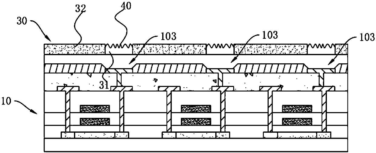
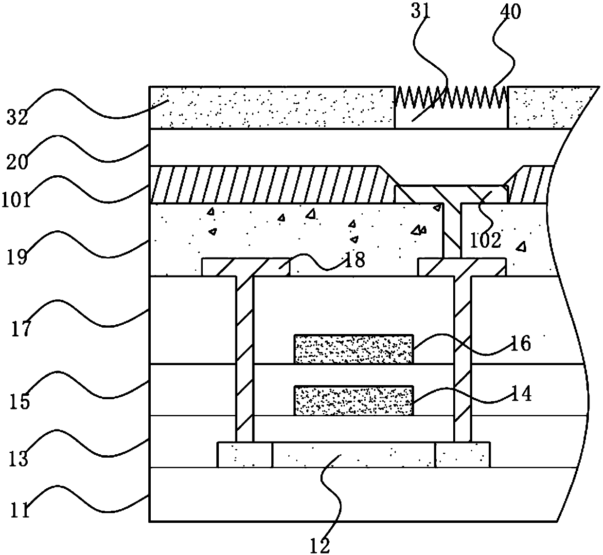
[0042] A kind of OLED display panel, such as figure 1 with figure 2 , the OLED display panel includes a display device board 10 , an encapsulation layer 20 disposed on the display device board 10 , and a color filter substrate 30 disposed on the encapsulation layer 20 .

[0043] Wherein, the display device panel 10 includes a display area 103 , the color filter substrate 30 includes a light-transmitting area 31 and a light-shielding area 32 formed by a black matrix, and the light-transmitting area 31 corresponds to the display area 103 .

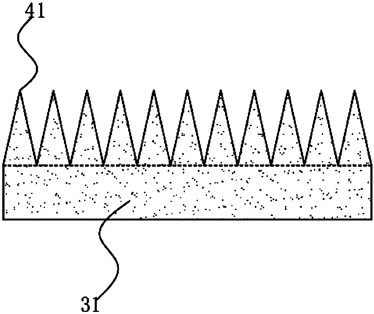
[0044] Wherein, the light-transmitting region 31 on the color filter substrate 30 is provided with a scattering structure 40 for scattering ambient light, and the scattering structure 40 includes a plurality of bumps 41, and the width of the bumps 41 is less than 600 nanometers .

[0045] By setting the scattering structure 40 at the light-transmitting region 31 of the color filter substrate 30, those skilled in the art know that when the...

Embodiment 2

[0057] A kind of OLED display panel, such as Figure 7 As shown, the only difference between it and the first embodiment lies in the shape of the scattering structure 40 .

[0058] Specifically, the shape of the longitudinal section of the bumps 41 is rectangular, the gaps 42 between the bumps are arranged, and the total area of ​​all the gaps 42 between the bumps 41 is 1 / 2 of the total area of ​​the light-transmitting region 31 0.2 to 0.5 times.

[0059] By making the gap 42 in the scattering structure 40 have an appropriate duty ratio, the anti-reflection effect of the scattering structure 40 on transmitted light is further improved, while the reflection effect on ambient light is reduced, and the contrast of the OLED display panel is improved.

[0060] It should be noted that, see Figure 8 to Figure 10 , Figure 8 to Figure 10 It is an experimental simulation diagram of the light transmittance of the color filter substrate 30 to light of different wavelengths when the g...

Embodiment 3

[0063] A kind of OLED display panel, such as Figure 11 As shown, the only difference between it and the first embodiment lies in the shape of the scattering structure 40 .

[0064] Specifically, the longitudinal section of the bumps 41 is trapezoidal.

[0065] It should be noted that the longitudinal section of the bumps 41 may be a straight trapezoid or an inverted trapezoid; the bumps 41 may be arranged in gaps or continuously.

[0066] It should be noted that, see Figure 12 to Figure 14 , Figure 12 to Figure 14 It is an experimental simulation diagram of the light transmittance of the color filter substrate 30 to light of different wavelengths when the longitudinal sections of the bumps 41 have different shapes.

[0067] Figure 12 is the simulation schematic diagram when there is no scattering structure; Figure 13 It is a simulation schematic diagram when the longitudinal section of the bump 41 is a positive trapezoid; Figure 14 It is a simulation schematic diag...


PUM


Abstract

The invention provides an OLED display panel and a preparation method thereof. The OLED display panel comprises a display device board, a packaging layer arranged on the display device board and a color film substrate arranged on the packaging layer; the display device board comprises a display area, the color film substrate comprises a light-transmitting zone and a light-shading zone, and the light-transmitting zone corresponds to the display area; and a scattering structure for scattering ambient light is arranged at the light-transmitting zone on the color film substrate and comprises a plurality of protruding particles. By arranging the scattering structure at the light-transmitting zone of the color film substrate, the certain transmittance increasing effect can be achieved on transmission light, the scattering structure is of a microstructure and has a optical grating like function, thus the transmittance of the color film substrate is increased, the reflecting function of the surface to light emitted by an OLED and the ambient light is reduced, and the contrast ratio of the OLED display panel is increased accordingly.

Description

technical field [0001] The invention relates to the field of display technology, in particular to an OLED display panel and a preparation method thereof. Background technique [0002] Polarizer (POL) can effectively reduce the reflectivity of the panel under strong light, but it will lose nearly 58% of the light output. For OLED, this greatly increases the burden on its life; on the other hand, the thickness of the polarizer is large and the material is brittle, which is not conducive to the development of dynamic bending products. [0003] At present, the technology of using color film substrate to replace polarizer in the industry can effectively improve the light output rate. However, for the color film substrate after spin-coating or inkjet printing, due to its own nature, it still has a negative impact on OLED self-luminescence and Ambient light has a high reflection effect, thereby reducing the contrast ratio of the OLED display panel. Contents of the invention [...

Claims


Application Information

Patent Timeline
Patent Type & Authority Applications(China)
IPC IPC(8): H01L51/52H01L27/32H01L21/77
CPCH10K59/12H10K50/854H10K59/1201H10K59/38H10K50/84H10K50/865H10K50/858H10K50/86H10K71/00
Inventor 陈泽升龚文亮
Owner WUHAN CHINA STAR OPTOELECTRONICS SEMICON DISPLAY TECH CO LTD
Why Eureka
Try Eureka