Novel 3D NAND memory device and method of forming same

A storage device and substrate technology, applied in read-only memory, static memory, information storage, etc., can solve the problems of 3D-NAND storage device block size increase, long data transmission time, low storage efficiency, etc.

Active Publication Date: 2019-04-26
YANGTZE MEMORY TECH CO LTD
View PDF4 Cites 49 Cited by
  • Summary
  • Abstract
  • Description
  • Claims
  • Application Information

AI Technical Summary

Problems solved by technology

The increase in the number of word line layers leads to a significant increase in the block size of 3D-NAND memory devices, which in turn leads to longer read and erase times, longer data transfer times, and lower storage efficiency

Method used


Image

  • Novel 3D NAND memory device and method of forming same
  • Novel 3D NAND memory device and method of forming same
  • Novel 3D NAND memory device and method of forming same

Examples


Embodiment Construction

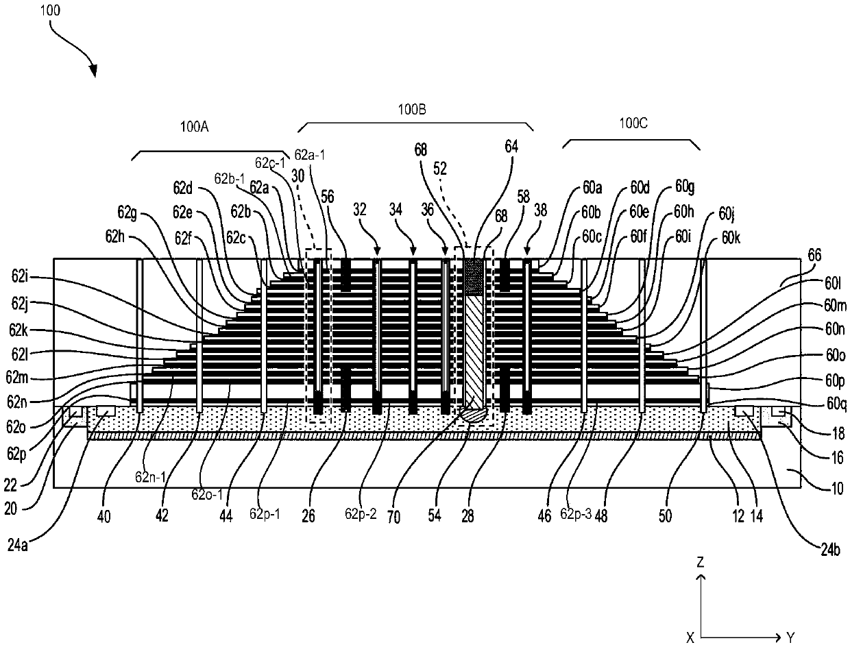
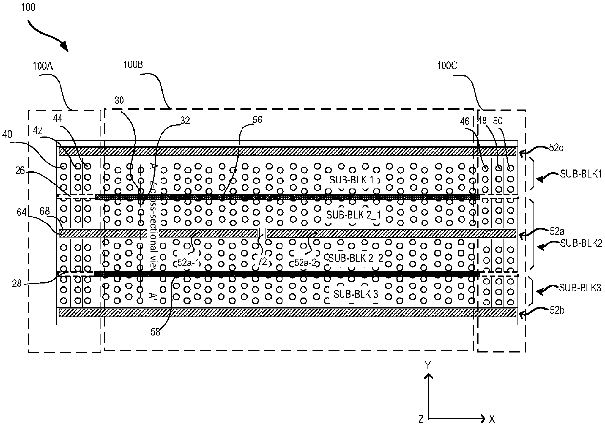
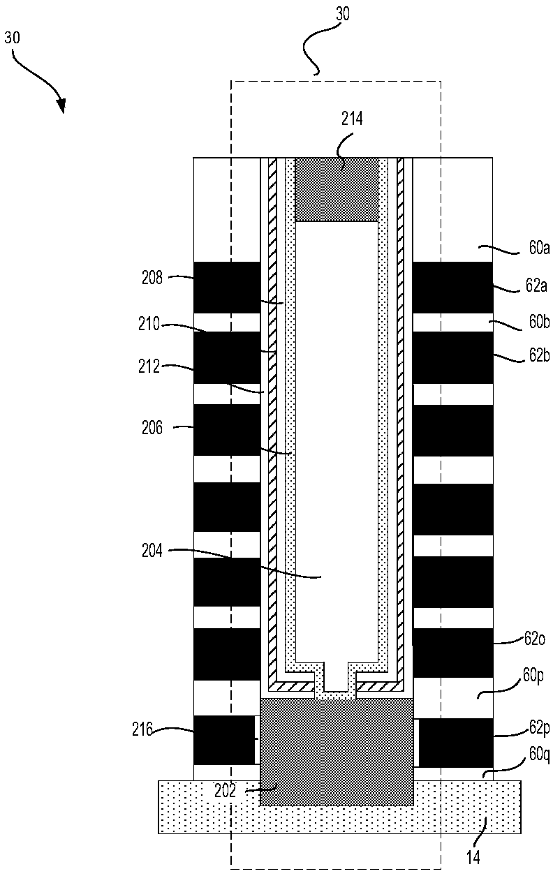
[0037] The following disclosure provides many different embodiments, or examples, for implementing different features of the presented subject matter. Specific examples of components and arrangements are described below to simplify the present disclosure. These are of course only examples and are not intended to be limiting. For example, forming a first feature over or on a second feature in the following description may include embodiments in which the first and second features are formed as features that can be in direct contact, and may also include embodiments in which , an additional feature may be formed between the first feature and the second feature such that the first feature and the second feature may not be in direct contact. Furthermore, the present disclosure may repeat reference numerals and / or letters in various examples. This repetition is for simplicity and clarity and does not in itself indicate a relationship between the various embodiments and / or configu...


PUM


Abstract

A 3D NAND memory device is provided and includes: a substrate, a bottom select gate (BSG) disposed over the substrate, a plurality of word lines disposed above the BSG and having a stepped configuration, and a plurality of insulation layers disposed between the substrate, the BSG, and the plurality of word lines. In the disclosed memory device, one or more first dielectric trenches are formed in the BSG and extend along the length of the substrate to separate the BSG into a plurality of sub-BSGs. Further, one or more common source regions are formed over the substrate and extend in the lengthdirection of the substrate. One or more common source regions also extend through the BSG, the plurality of word lines, and the plurality of insulating layers.

Description

Background technique [0001] As feature sizes of devices in integrated circuits shrink to the limits of common memory cell technology, designers have sought techniques for stacking multiple planes of memory cells to achieve greater storage capacity and achieve lower cost per bit. [0002] 3D-NAND memory devices are exemplary devices that stack multiple planes of memory cells to achieve greater storage capacity and achieve lower cost per bit. 3D-NAND technology is moving towards high density and high capacity, especially from 64L to 128L architecture, and the number of word line layers (or gate control layers) in the vertical direction perpendicular to the substrate has increased significantly. The increase in the number of word line layers leads to a significant increase in the block size of 3D-NAND memory devices, which in turn leads to longer read and erase times, longer data transfer times, and lower storage efficiency. Contents of the invention [0003] The inventive con...

Claims


Application Information

Patent Timeline
Patent Type & Authority Applications(China)
IPC IPC(8): H01L27/1158
CPCH10B41/20H10B43/23G11C16/0483G11C16/14H10B41/10H10B41/50H10B43/10H10B43/50H10B41/27H10B43/27H01L21/823475H01L21/0276H01L21/31116H01L21/31144H01L23/528H01L29/0847H01L29/1037H10B43/35
Inventor 宋雅丽肖莉红王明
Owner YANGTZE MEMORY TECH CO LTD
Why Eureka
Try Eureka