Zero common-mode voltage space vector modulation method for parallel three-level converters in photovoltaic grid-connected applications
A space vector modulation, common mode voltage technology, applied in photovoltaic power generation, single grid parallel feeding arrangement, etc., can solve the problems of low waveform quality and large output current harmonics of the converter, so as to ensure the differential mode and common mode circulating current. , the effect of improving the quality of output current
- Summary
- Abstract
- Description
- Claims
- Application Information
AI Technical Summary
Problems solved by technology
Method used
Image
Examples
specific Embodiment approach 1
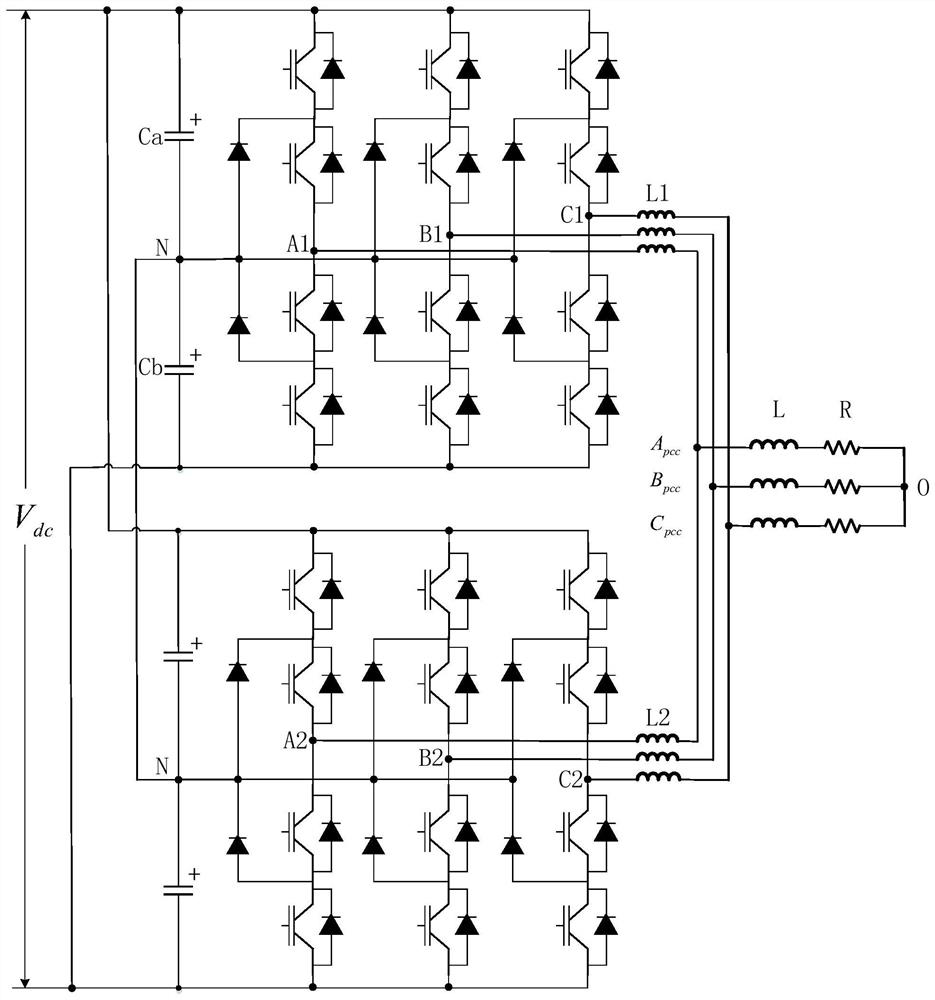
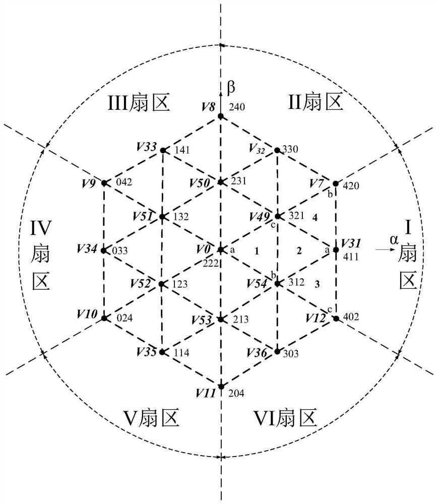
[0078] According to the above analysis, in this embodiment, the zero-common-mode voltage space vector modulation method suitable for parallel three-level converters in photovoltaic grid-connected applications, the parallel three-level converters are regarded as a five-level system. Among all five-level fundamental vectors of the level system, 19 fundamental vectors corresponding to zero common-mode voltage are selected. Then, based on these 19 zero common-mode voltage vectors, the adjacent three zero common-mode voltage vectors are formed into an equilateral triangle in the vector space of the five-level system. The vector space is partitioned to obtain 24 cells, which can be obtained as figure 2 The zero common-mode voltage vector space is shown.
[0079] Area division steps:
[0080] With a zero common-mode voltage vector V located at the center of the vector space 0 The point is the center of the circle, the center of the circle is the origin, the αβ plane rectangular c...
specific Embodiment approach 2
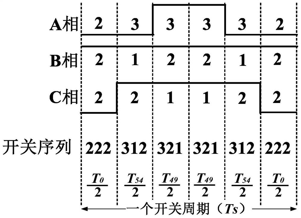
[0117] Embodiment 2: This embodiment is a further description of the zero common-mode voltage space vector modulation method for parallel three-level converters in photovoltaic grid-connected applications described in Embodiment 1. In this embodiment, it is assumed that the reference The vector is in figure 2 Medium I sector 1 cell, then the three vertex vectors corresponding to the cell are V 0 , V 54 , V 49 , the corresponding vector action times are respectively T 0 , T 54 , T 49 , then the corresponding five-level switch sequence is: 222-312-321-|-321-312-222. Corresponding the sequence with the vector action time, a schematic diagram of the switching sequence within a switching cycle is obtained, as shown in image 3 shown.
[0118] Since the circulating current can only ensure the normal operation of the system, there are two basic principles: one is to make the circulating current return to the value at the beginning of the cycle at the end of a switching cycle,...
PUM
 Abstract
Description
Claims
Application Information


