Multi-band time-dividing optical exposure device and method

An optical exposure and multi-band technology, which is applied in photolithography exposure devices, microlithography exposure equipment, and secondary processing of printed circuits, etc., can solve the problems of inability to distinguish and control different wavelengths, production discounts, and low work efficiency. To achieve the effect of sufficient photochemical reaction, accelerated exposure speed and high definition

Active Publication Date: 2019-05-07
JIANGSU YSPHOTECH INTERGRATED CIRCUIT EQUIP CO LTD
View PDF5 Cites 1 Cited by
  • Summary
  • Abstract
  • Description
  • Claims
  • Application Information

AI Technical Summary

Problems solved by technology

In the above two methods, because the mercury lamp light source is a single light source with mixed wavelengths, different wavelengths cannot be distinguished and controlled during exposure, so it is impossible to achieve exposure of different wavelengths in a certain time sequence; the mixed light source can realize control of different wavelengths according to requirements. The light source is lit according to a certain time sequence, but because a set of optical system is used as a whole, repeated exposures need to be performed many times, the production capacity will be greatly reduced, and the work efficiency will be low

Method used


Image

  • Multi-band time-dividing optical exposure device and method
  • Multi-band time-dividing optical exposure device and method
  • Multi-band time-dividing optical exposure device and method

Examples


Embodiment 1

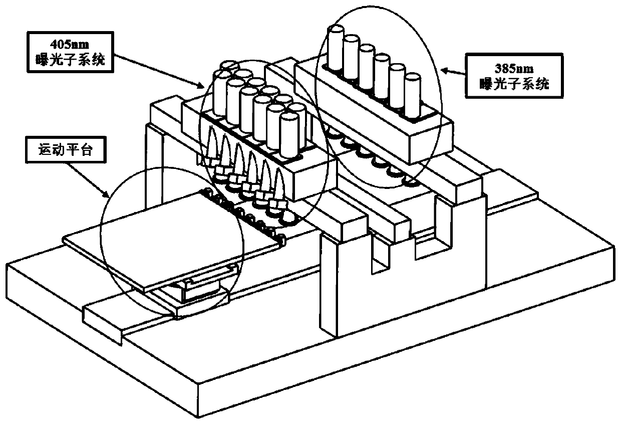
[0041] This embodiment provides a multi-band and time-segmented exposure device. The multi-band optical exposure device includes at least two groups of exposure subsystems, and each group of exposure subsystems matches light sources of different wavelength ranges and spatial light modulators corresponding to different wavelength ranges. Each group of exposure subsystems is arranged at different positions in the scanning direction of the multi-waveband optical exposure device according to the time interval required for the light source of the matched wavelength to expose the substrate to be exposed.

[0042] refer to figure 1In this embodiment, the multi-band and time-segmented exposure device includes two sets of exposure subsystems, and each set of exposure subsystems matches single-wavelength light sources of different wavelengths. For the convenience of description, the two sets of exposure subsystems are respectively recorded as exposure System 1 and exposure subsystem 2; ...

Embodiment 2

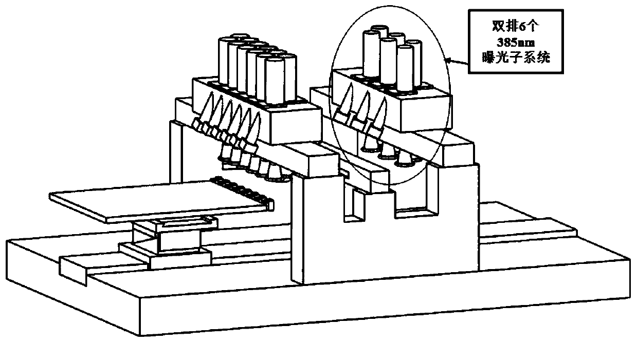
[0050] This embodiment provides a multi-band and time-segmented exposure device. The multi-band optical exposure device includes at least two groups of exposure subsystems, and each group of exposure subsystems matches light sources of different wavelength ranges and spatial light modulators corresponding to different wavelength ranges. Each group of exposure subsystems is arranged at different positions in the scanning direction of the multi-waveband optical exposure device according to the time interval required for the light source of the matched wavelength to expose the substrate to be exposed.

[0051] The matching of each group of exposure subsystems to light sources of different wavelength ranges includes: each group of exposure subsystems matching different wavelength single-wavelength light sources and / or each group of exposure subsystems matching integrated light sources in different wavelength ranges.

[0052] refer to figure 2 In this embodiment, the multi-band an...

Embodiment 3

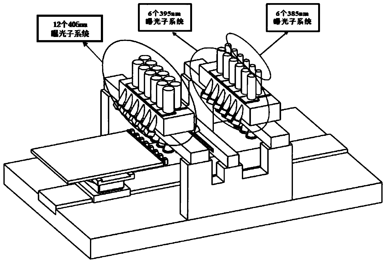
[0067] This embodiment provides a multi-band and time-segmented exposure device. The multi-band optical exposure device includes at least two groups of exposure subsystems, and each group of exposure subsystems matches light sources of different wavelength ranges and spatial light modulators corresponding to different wavelength ranges. Each group of exposure subsystems is arranged at different positions in the scanning direction of the multi-waveband optical exposure device according to the time interval required for the light source of the matched wavelength to expose the substrate to be exposed.

[0068] The matching of each group of exposure subsystems to light sources of different wavelength ranges includes: each group of exposure subsystems matching different wavelength single-wavelength light sources and / or each group of exposure subsystems matching integrated light sources in different wavelength ranges.

[0069] refer to image 3 In this embodiment, the multi-band exp...


PUM


Abstract

The invention discloses a multi-band time-dividing optical exposure device and method, and belongs to the technical field of printed circuit boards. According to the method, light sources with different wavelengths are separated, on a set of photoelectric exposure device, a plurality exposure sub systems are adaptive, each exposure sub system is matched with the light sources with different wavelengths and spatial light modulators corresponding to different wavelength ranges to perform multi-time sequencing exposure for a substrate to be exposed, the exposure sub systems are arranged at intervals at different positions in the multi-band optical exposure device scanning direction according to the time required when exposure of the substrate to be exposed is performed by employing the lightsources with the matching wavelengths to allow different exposure sub systems to allow different exposure sub systems to have a certain time interval in the photochemical reaction at different depthsof the material or with different photoinitiators to allow the photochemical reaction to be more full and allow the exposed images to be better in glossiness and clearer.

Description

technical field [0001] The invention relates to a multi-band and time-divided optical exposure device and method, belonging to the technical field of printed circuit boards. Background technique [0002] Composite photosensitive material is a photosensitive material that can produce photochemical reactions to light sources of various wavelengths. In the printed circuit board (Printed Circuit Board, PCB) industry in the field of integrated circuits, the light-cured solder resist used in the solder resist process Ink, because it is doped with photoinitiators of various wavelengths, is a typical composite photosensitive material. The basic composition of PCB solder resist ink is: prepolymer, reactive diluent, photoinitiator, pigment, additives, etc. In the solder resist process, the ultraviolet (ultra-violet, UV) curing of PCB solder resist ink relies on the photoinitiator to absorb the radiation energy of the ultraviolet light source to form free radicals, triggering the cros...

Claims


Application Information

Patent Timeline
Patent Type & Authority Applications(China)
IPC IPC(8): G03F7/20H05K3/28
Inventor 陈海巍宋志尚李显杰钱聪程珂徐敏王伟王军华茆晓华吴长江刘世林袁征蒯多杰
Owner JIANGSU YSPHOTECH INTERGRATED CIRCUIT EQUIP CO LTD
Why Eureka
Try Eureka