Display panel, manufacturing method thereof, and display device

A technology for display panels and substrates, applied in the field of display devices, display panels and their manufacturing, can solve the problems of inability to realize full-screen in-screen fingerprint recognition and insufficient pixel aperture ratio, so as to increase the pixel aperture ratio and realize in-screen fingerprint recognition , the effect of promoting development

Active Publication Date: 2021-01-26
BOE TECH GRP CO LTD +1
View PDF8 Cites 0 Cited by
  • Summary
  • Abstract
  • Description
  • Claims
  • Application Information

AI Technical Summary

Problems solved by technology

[0006] The purpose of the present invention is to propose an improved display panel structure, which solves the technical problem that the pixel aperture ratio of the display panel is not high enough to realize the in-screen fingerprint recognition of the full screen

Method used


Image

  • Display panel, manufacturing method thereof, and display device
  • Display panel, manufacturing method thereof, and display device
  • Display panel, manufacturing method thereof, and display device

Examples


Embodiment Construction

[0023] Various aspects and features of the present disclosure are described herein with reference to the accompanying drawings. The nature of the invention will become apparent from the following description of preferred forms of embodiment given as non-limiting examples with reference to the accompanying drawings.

[0024] This specification may use the phrases "in one embodiment," "in another embodiment," "in yet another embodiment," or "in other embodiments," which may refer to the same or one or more of the different embodiments. In a specific embodiment, an element appearing in a singular form does not exclude that it may appear in a plural (plural) form.

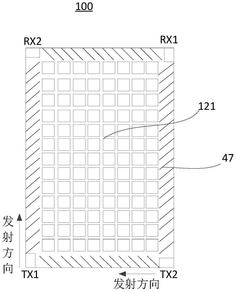
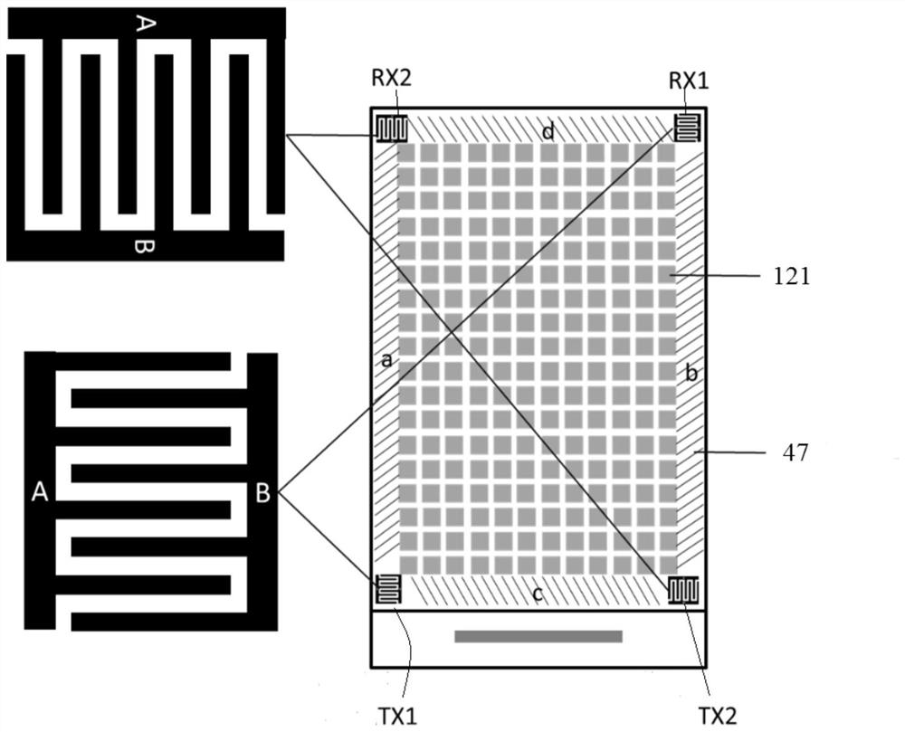
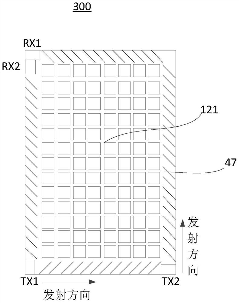
[0025] figure 1 The structure of the display panel 100 according to the embodiment of the present invention is shown.

[0026] to combine Figure 4 , the display panel 100 includes a base substrate 41 and a piezoelectric sensing layer 43 formed on the base substrate.

[0027] The base substrate 41 is, for example,...


PUM


Abstract

The invention relates to a display panel, a manufacturing method thereof and a display device. The display panel comprises a substrate and a piezoelectric induction layer formed on the substrate, andis characterized in that the piezoelectric induction layer includes; a signal transmitting unit configured to transmit a surface acoustic wave signal; a signal receiving unit configured to receive a surface acoustic wave signal; a plurality of wire grid arrays configured to reflect the surface acoustic wave signals transmitted by the signal transmitting unit to the signal receiving unit; And the semiconductor layer array which is arranged in an area enclosed by the plurality of groups of wire grid arrays, wherein the plurality of groups of wire grid arrays are arranged to enable reflected surface acoustic wave signals to spread over the semiconductor layer array and then reach the signal receiving unit. According to the invention, the in-screen fingerprint identification of the full-screenpanel can be realized.

Description

technical field [0001] The present invention relates to the field of display technology, in particular to a display panel, a manufacturing method thereof, and a display device. Background technique [0002] The existing fingerprint identification technology usually detects the reflected light of the finger, and judges whether the corresponding position is a fingerprint valley or a fingerprint ridge according to the difference in light intensity of the reflected light between the fingerprint valley and the fingerprint ridge, thereby forming a fingerprint image at the corresponding position. [0003] Chinese Patent Publication No. 108052930 (CN108052930A) proposes an array substrate that can be used for fingerprint recognition. The array substrate includes: a base substrate; a piezoelectric sensing layer formed on the base substrate; a surface acoustic wave excitation electrode and a surface acoustic wave receiving electrode formed on the piezoelectric sensing layer; and a sur...

Claims


Application Information

Patent Timeline
Patent Type & Authority Patents(China)
IPC IPC(8): G06K9/00H01L27/32
Inventor 吕振华尤杨邱云曲连杰贵炳强王慧娟
Owner BOE TECH GRP CO LTD
Why Eureka
Try Eureka