Electro-optical device

a technology of optical devices and optical components, applied in the field of optical components, can solve the problems of increasing the number of production processing steps, increasing increasing the number of layers in the multi-layer structure and the number of contact holes, so as to achieve the effect of increasing the capacitan

Active Publication Date: 2006-02-23
138 EAST LCD ADVANCEMENTS LTD
View PDF17 Cites 14 Cited by
  • Summary
  • Abstract
  • Description
  • Claims
  • Application Information

AI Technical Summary

Benefits of technology

[0055] In this exemplary embodiment, the contact hole via which the light-shielding film and the capacitance line are connected to each other is covered with the data line, and thus steps formed on the surface of the alignment film near the contact hoe can be reduced. Furthermore, it is also possible to increase the capacitance by using the light-shielding film as the capacitor electrode.

Problems solved by technology

The use of the intermediate conductive layer described above results in not only an increase in the number of production processing steps, but also increases in the number of layers formed in the multilayer structure and the number of contact holes.
As a result, the multilayer structure becomes more complicated.
Thus, as the pixel pitch is reduced, it becomes more difficult to form the above-described storage capacitor and to find areas in which to form contact holes.
Another problem due to the increase in the number of contact holes as a result of the formation of the intermediate conductive layer is that the contact holes create steps in an interlayer insulating film above the contact holes, and thus create steps in the pixel electrode and in an alignment film formed on the pixel electrode.
The steps formed in the alignment film, in the vicinity of the pixel electrode, can make it impossible to correctly orient an electro-optical material such as a liquid crystal, which can cause an operational failure.
As a result, a reduction in contrast and thus a great reduction in image quality occur.

Method used


Image

  • Electro-optical device
  • Electro-optical device
  • Electro-optical device

Examples


first exemplary embodiment

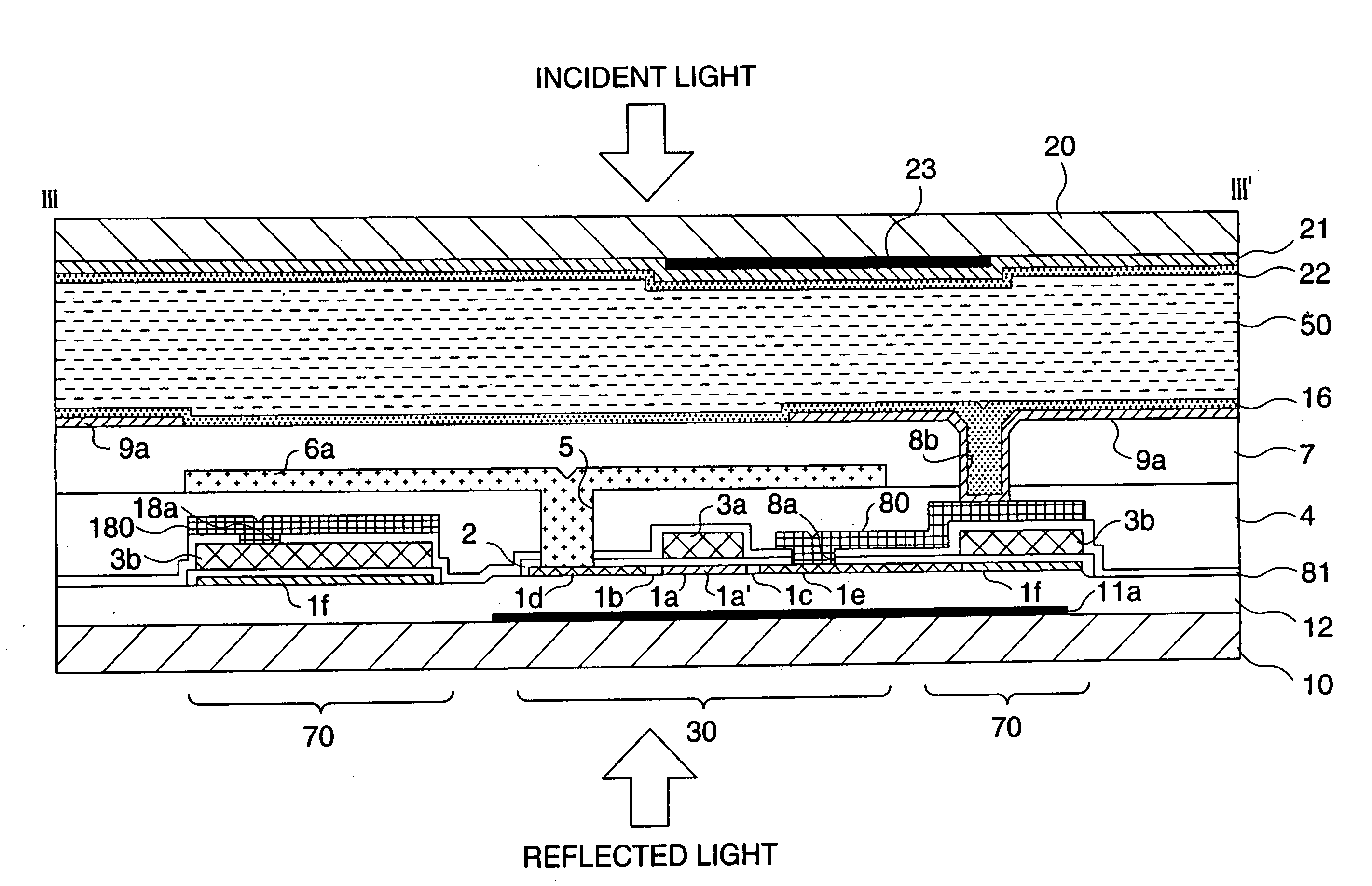
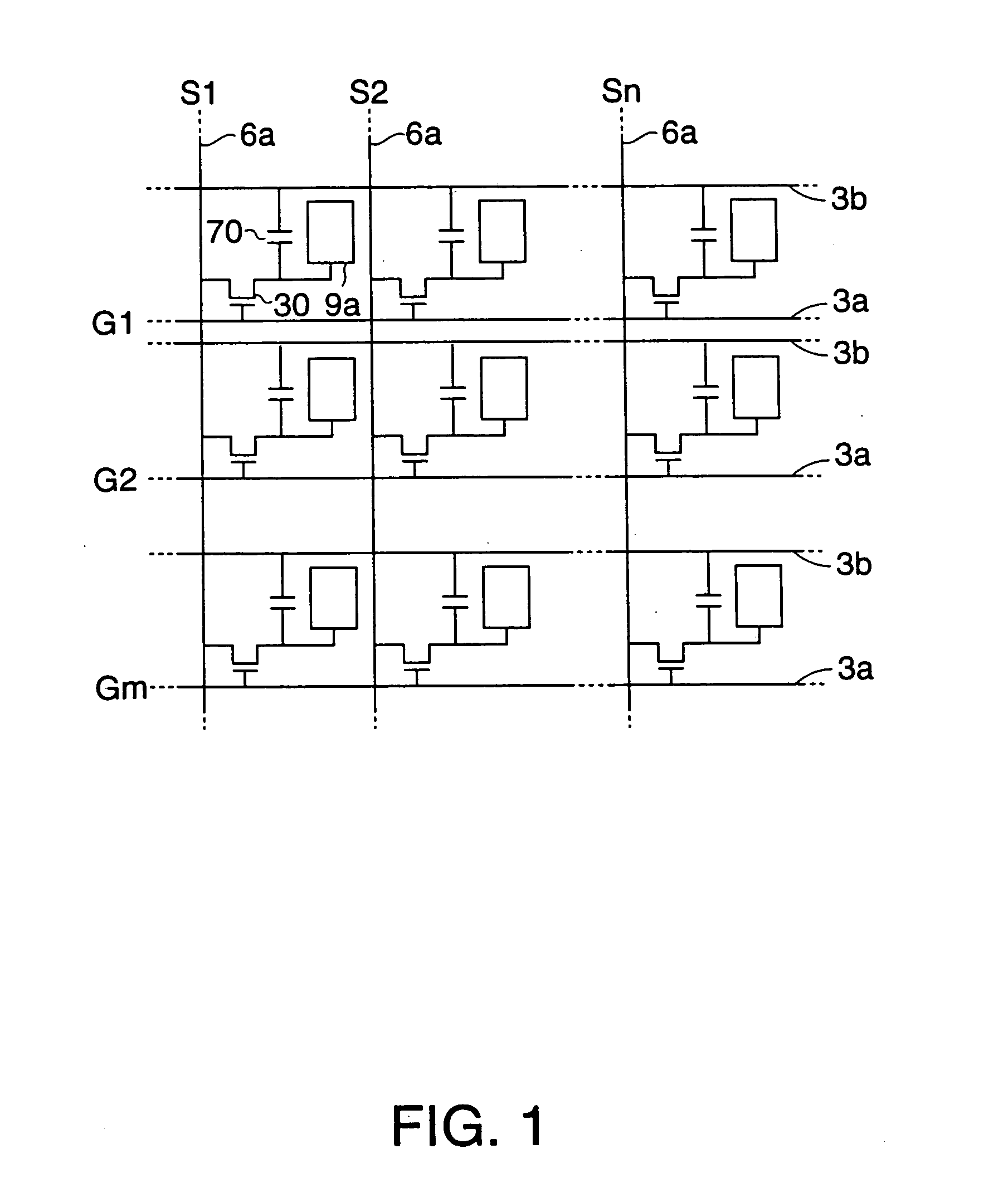
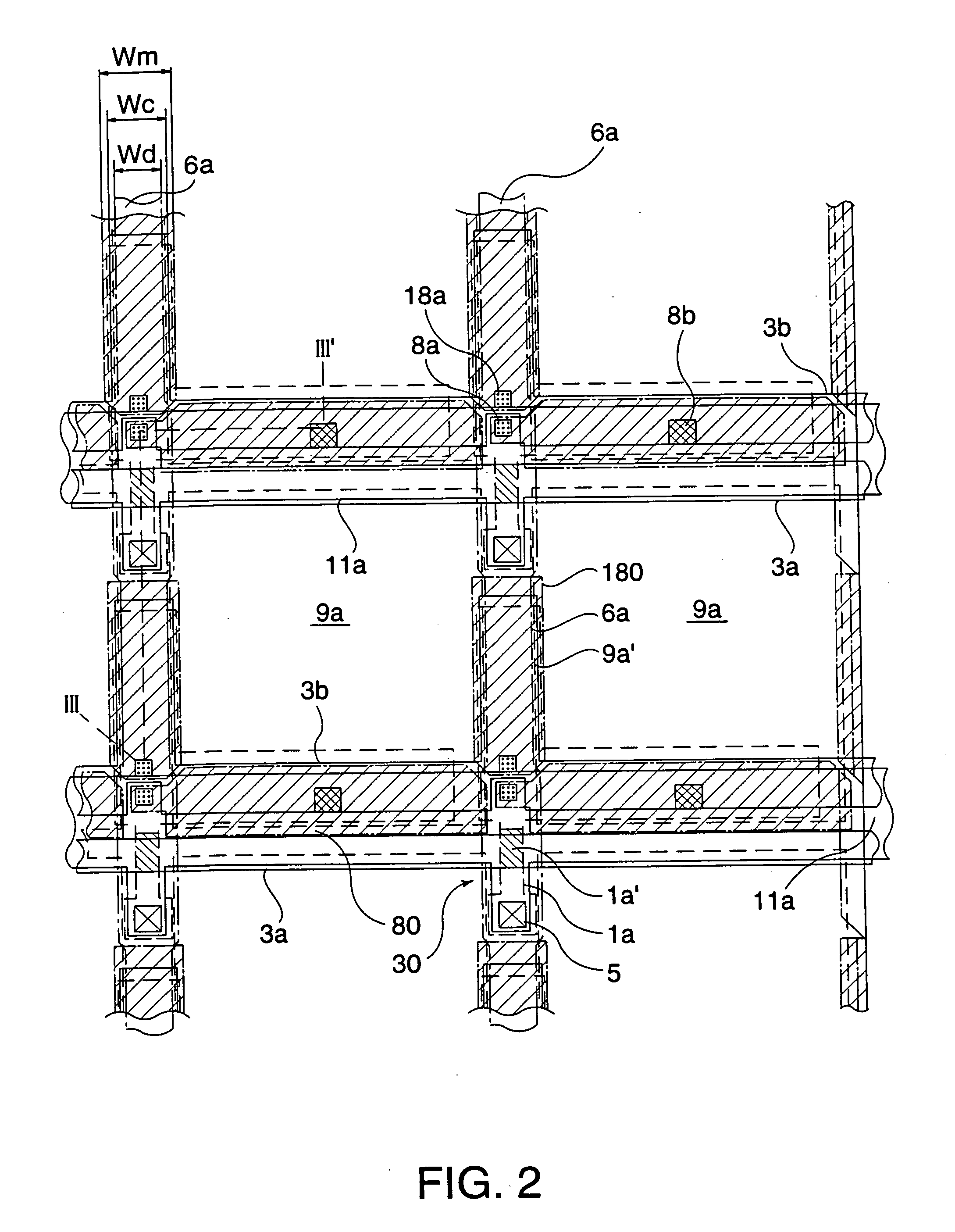
[0071] The structure of an electro-optical device in the form of a liquid crystal device according to a first exemplary embodiment of the present invention is described below with reference to FIGS. 1 to 4(B). FIG. 1 illustrates an equivalent circuit of various elements and interconnections of respective pixels arranged in a matrix fashion in an image display area of the electro-optical device. FIG. 2 is a plan view illustrating some pixels formed at adjacent locations on a TFT array substrate on which data lines, scanning lines, and pixel electrodes are also formed. FIG. 3 is a cross-sectional view taken along line III-III′ of FIG. 2. In FIG. 3, in order to provide an easily understandable view, the respective layers and members are displayed in different magnification ratios. FIG. 4(A)-(B) are plan views illustrating in an enlarged fashion a part of a pattern of a capacitance line and a scanning line according to the present embodiment (FIG. 4(A)) wherein a capacitance line and a ...

second exemplary embodiment

[0134] The structure of an electro-optical device in the form of a liquid crystal device according to a second exemplary embodiment of the present invention is described below with reference to FIGS. 7 and 8. FIG. 7 is a plan view illustrating some pixels formed at adjacent locations on a TFT array substrate on which data lines, scanning lines, and pixel electrodes are also formed. FIG. 8 is a cross-sectional view taken along line VIII-VIII′ of FIG. 7. In FIG. 8, in order to provide an easily understandable view, the respective layers and members are displayed in different magnification ratios.

[0135] As shown in FIGS. 7 and 8, the second embodiment is similar to the first embodiment except that the first intermediate layer 80 and the second intermediate layer 180 in the first embodiment are combined into a single layer as an intermediate conductive layer 80′ in the form of an L shape for each pixel in the second embodiment, and, correspondingly, the contact hole 18a used in the fir...

third exemplary embodiment

[0137] The structure of an electro-optical device in the form of a liquid crystal device according to a third exemplary embodiment of the present invention is described below with reference to FIGS. 9 and 10. FIG. 9 is a plan view illustrating some pixels formed at adjacent locations on a TFT array substrate on which data lines, scanning lines, and pixel electrodes are also formed. FIG. 10 is a cross-sectional view taken along line X-X′ of FIG. 9. In FIG. 10, in order to provide an easily understandable view, the respective layers and members are displayed in different magnification ratios.

[0138] In FIGS. 9 and 10, similar constituent elements to those in the first embodiment described above with reference to FIGS. 2 and 3 or to those in the second embodiment described above with reference to FIGS. 7 and 8 are denoted by similar reference numerals and they are not described in further detail herein.

[0139] In this third embodiment, the intermediate conductive layer 80′ is disposed ...


PUM

PropertyMeasurementUnit
distanceaaaaaaaaaa
thicknessaaaaaaaaaa
thicknessaaaaaaaaaa

Abstract

An electro-optical device includes a substrate on which a TFT, a data line, a scanning line, a capacitance line, a first intermediate conductive layer, a second intermediate conductive layer, and a pixel electrode are formed. A first contact hole, via which the drain of the TFT and the first intermediate conductive layer are connected to each other, is formed in an area which overlaps, in plan view, with the data line. The above-described structure of this electro-optical device, which includes the intermediate conductive layer disposed between the pixel electrode and the pixel switching TFT, allows an increase in the pixel aperture ratio and also an increase in the storage capacitance. Besides, degradation in the quality of a displayed image due to steps formed, in the vicinity of the pixel electrode, on the surface of an alignment film is minimized.

Description

[0001] This is a Division of application Ser. No. 09 / 809,207 filed Mar. 16, 2001. The entire disclosure of the prior application is hereby incorporated by reference herein in its entirety.BACKGROUND OF THE INVENTION [0002] 1. Field of Invention [0003] The present invention relates to an electro-optical device using an active matrix addressing method. More particularly, the present invention relates to an electro-optical device including an intermediate conductive layer which serves to provide a good electrical connection between a pixel electrode and a pixel switching thin film transistor (hereinafter also referred to as a TFT), and which is formed as one of layer of a multilayer structure formed on a substrate. [0004] 2. Description of Related Art [0005] In a conventional electro-optical device using TFTs as active matrix addressing elements, when a scanning signal is applied to the gate electrode of a TFT via a scanning line, the TFT is turned on, and an image signal applied via a...

Claims


Application Information

Patent Timeline
Patent Type & Authority Applications(United States)
IPC IPC(8): G02F1/136G02F1/1362G02F1/1368G09F9/30H01L21/768H01L29/786
CPCG02F1/136213G02F1/1368G02F1/136227
Inventor MURADE, MASAO
Owner 138 EAST LCD ADVANCEMENTS LTD
Why Eureka
Try Eureka