

Electro-optical device and electronic apparatus
a technology of optical devices and electronic devices, applied in the direction of static indicating devices, discharge tubes, instruments, etc., can solve the problem of difficulty in increasing the pixel aperture ratio further, and achieve the effect of high luminance level
- Summary
- Abstract
- Description
- Claims
- Application Information
AI Technical Summary
Benefits of technology
Problems solved by technology
Method used
Image

Examples
embodiment 1
Whole Configuration
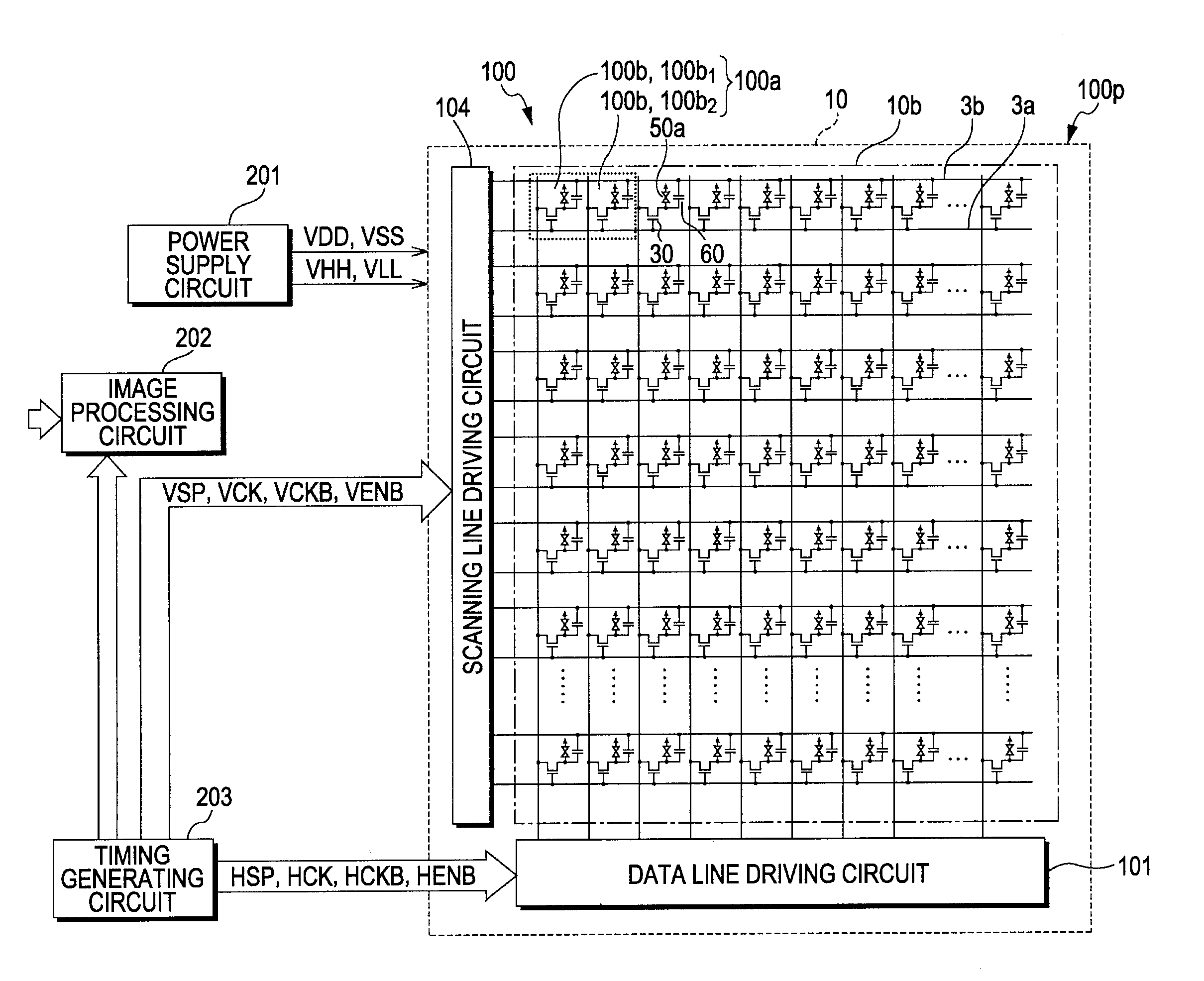
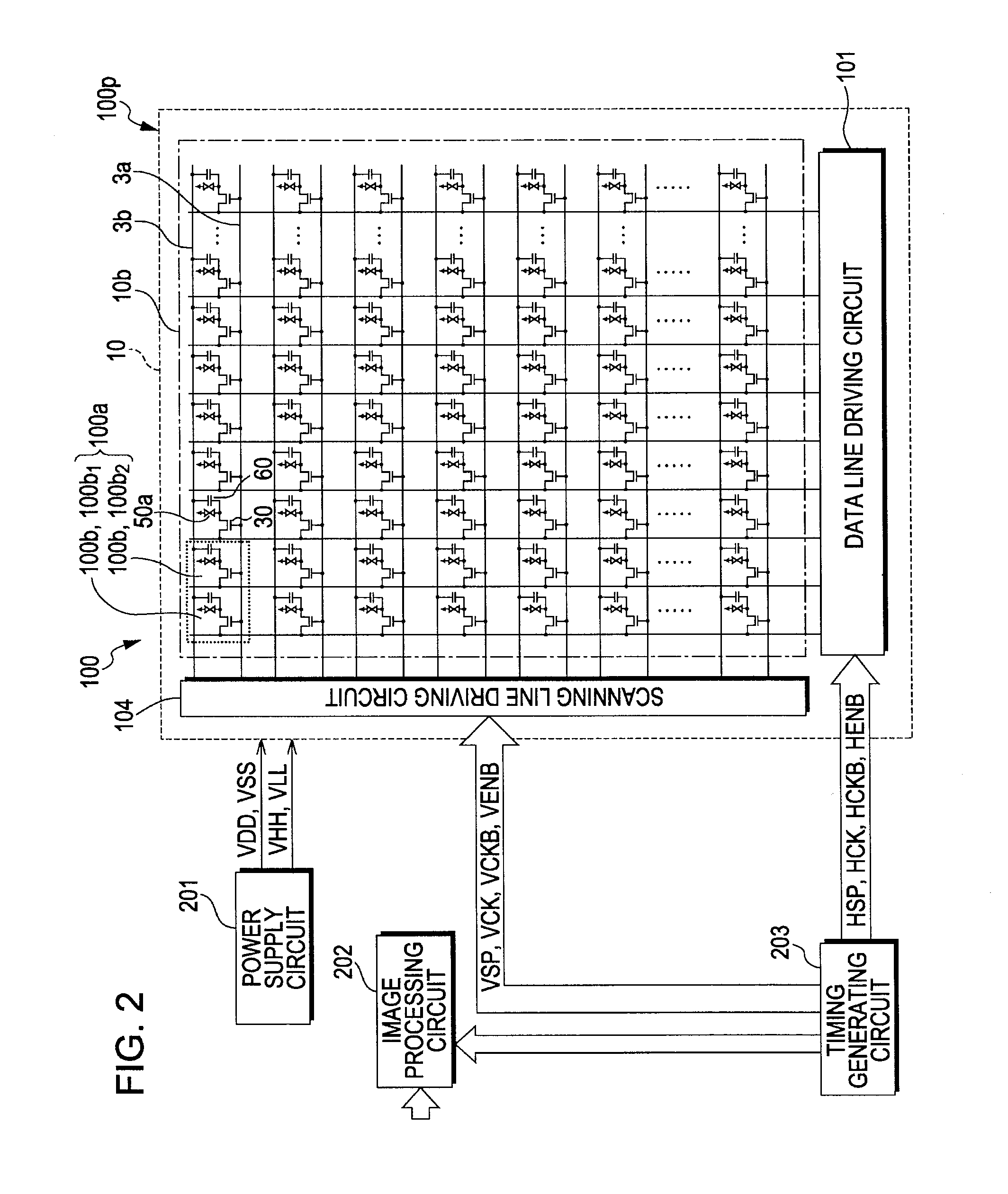
[0045]FIG. 2 is a block diagram showing the electrical configuration of an electro-optical device according to an embodiment of the invention. As shown in FIG. 2, the electro-optical device 100 is configured mainly by a liquid crystal panel 100p, an image processing circuit 202, a timing generating circuit 203, and a power supply circuit 201. The image processing circuit 202, the timing generating circuit 203, and the power supply circuit 201 are configured by an IC or the like that is mounted on a flexible substrate (not shown) connected to the liquid crystal panel 100p. In the timing generating circuit 203, a dot clock used for driving pixels 100a (sub pixels 100b) of the liquid crystal panel 100p is generated. In addition, based on the dot clock, clock signals VCK and HCK, inverted clock signals VCKB and HCKB, and transfer stating pulses HSP and VSP are generated. When input image data is input from the outside, the image processing circuit 202 generates an ima...
embodiment 2
[0065]FIG. 6 is a diagram showing a two-dimensional arrangement of pixels (sub pixels) of an electro-optical device 100 according to Embodiment 2 of the invention. Since a basic configuration of this embodiment is the same as that of Embodiment 1, a same reference sign is attached to a part common to Embodiment 1, and a description thereof is omitted here.
[0066]As shown in FIG. 6, in the electro-optical device 100 according to this embodiment, one pixel 100a is also configured by two sub pixels 100b. In this embodiment, in any of the plurality of pixels 100a, one sub pixel (a first sub pixel 100b1) between two sub pixels 100b is a color sub pixel corresponding to red color (R), and the other sub pixel (a second sub pixel 100b2) is a color sub pixel corresponding to green color (G).
[0067]In addition, a stripe arrangement is employed as the color arrangement of the electro-optical device 100 according to this embodiment. Accordingly, when directions perpendicular to each other are set...
embodiment 3
[0072]FIG. 7 is a diagram showing a two-dimensional arrangement of pixels (sub pixels) of an electro-optical device 100 according to Embodiment 3 of the invention. Since a basic configuration of this embodiment is the same as that of Embodiment 1, a same reference sign is attached to a part common to Embodiment 1, and a description thereof is omitted here.
[0073]As shown in FIG. 7, in the electro-optical device 100 according to this embodiment, one pixel 100a is also configured by two sub pixels 100b. In this embodiment, in any of the plurality of pixels 100a, one sub pixel (a first sub pixel 100b1) between two sub pixels 100b is a color sub pixel corresponding to red color (R), and the other sub pixel (a second sub pixel 100b2) is a color sub pixel corresponding to green color (G). In addition, in any of the plurality of pixels 100a, the first sub pixel 100b1 and the second sub pixel 100b2 have a same size.
[0074]Here, a delta arrangement is employed as color arrangement of the elect...
PUM
 Abstract
Description
Claims
Application Information