OLED display device and preparation method of TFT array substrate

A technology for display devices and substrates, which is applied in the manufacture of semiconductor/solid-state devices, electrical components, and electrical solid-state devices, etc., can solve the problems of reducing the channel width of the driving tube, reducing the parasitic effect of the switching tube, and increasing the yellow light process, etc. Achieve the effect of improving the display effect and improving the pixel aperture ratio

Inactive Publication Date: 2020-05-22
SHENZHEN CHINA STAR OPTOELECTRONICS SEMICON DISPLAY TECH CO LTD
View PDF4 Cites 15 Cited by
  • Summary
  • Abstract
  • Description
  • Claims
  • Application Information

AI Technical Summary

Problems solved by technology

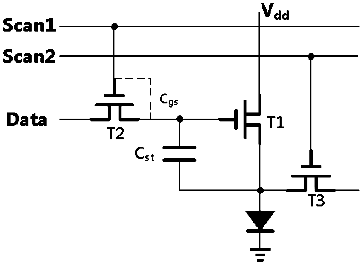
[0005] The embodiment of the present application provides a method for preparing an OLED display device and a TFT array substrate, which can reduce the parasitic effect of the switching tube and reduce the channel width of the driving tube, so as to solve the problem of the existing OLED display device and the preparation method of the TFT array substrate. In the 3T1C pixel circuit, the use of the top gate self-aligned amorphous oxide TFT structure will introduce a light-shielding layer, adding an additional yellow light process, but the technical problem of not increasing the on-state current of the device

Method used


Image

  • OLED display device and preparation method of TFT array substrate
  • OLED display device and preparation method of TFT array substrate
  • OLED display device and preparation method of TFT array substrate

Examples


Embodiment Construction

[0029] The technical solutions in the embodiments of the present application will be clearly and completely described below in conjunction with the drawings in the embodiments of the present application. Apparently, the described embodiments are only some of the embodiments of this application, not all of them. Based on the embodiments in this application, all other embodiments obtained by those skilled in the art without making creative efforts belong to the scope of protection of this application.

[0030] In the description of the present application, it should be understood that the terms "center", "longitudinal", "transverse", "length", "width", "thickness", "upper", "lower", "front", " Orientation indicated by rear, left, right, vertical, horizontal, top, bottom, inside, outside, clockwise, counterclockwise, etc. The positional relationship is based on the orientation or positional relationship shown in the drawings, which is only for the convenience of describing the a...


PUM


Abstract

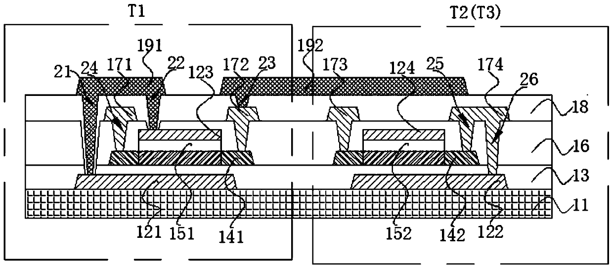
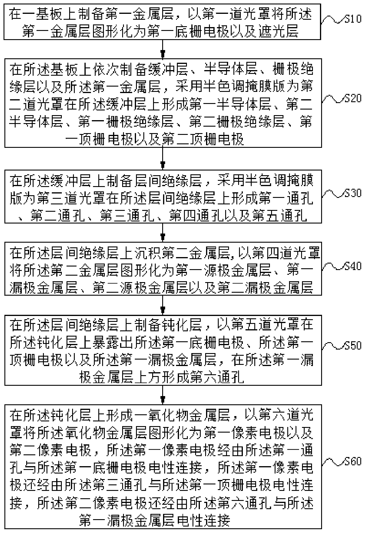
The invention discloses an OLED display device, which comprises an OLED pixel driving circuit. The OLED pixel driving circuit comprises a first thin film transistor (T1), a second thin film transistor(T2), a third thin film transistor (T3), a storage capacitor (Cst) and an organic light emitting diode, wherein the first thin film transistor (T1) is a double-gate oxide thin film transistor, and the second thin film transistor (T2) and the third thin film transistor (T3) are top gate self-aligned oxide thin film transistors. The invention further discloses a preparation method of the TFT arraysubstrate. The TFT array substrate is used for preparing the OLED display device.

Description

technical field [0001] The present application relates to the field of display technology, in particular to an OLED display device and a method for preparing a TFT array substrate. Background technique [0002] Organic light emitting diode (Organic Light Emitting Display, OLED) display device has self-illumination, low driving voltage, high luminous efficiency, short response time, high definition and contrast, nearly 180° viewing angle, wide operating temperature range, and can realize flexible display and With many advantages such as large-area full-color display, it is recognized by the industry as a display device with the most potential for development. [0003] In the current OLED pixel drive circuit, a 3T1C (that is, a structure of three thin film transistors plus a capacitor) circuit composed of a top-gate self-aligned amorphous oxide TFT is generally used to drive the OLED to emit light. Light is very sensitive, and the threshold voltage of the device will decrease...

Claims


Application Information

Patent Timeline
Patent Type & Authority Applications(China)
IPC IPC(8): H01L27/12H01L27/32H01L21/77
CPCH01L27/1251H01L27/1225H01L27/1288H10K59/1213H01L29/78648H01L29/7869H10K59/126H10K59/1201H10K59/131H10K59/1216
Inventor 张乐陶张晓星
Owner SHENZHEN CHINA STAR OPTOELECTRONICS SEMICON DISPLAY TECH CO LTD
Why Eureka
Try Eureka