Manufacturing method of semiconductor device structure
A technology of device structure and manufacturing method, applied in the field of semiconductor device structure and its manufacturing, can solve the problems of unsatisfactory aspect and the like
- Summary
- Abstract
- Description
- Claims
- Application Information
AI Technical Summary
Problems solved by technology
Method used
Image

Examples
Embodiment Construction
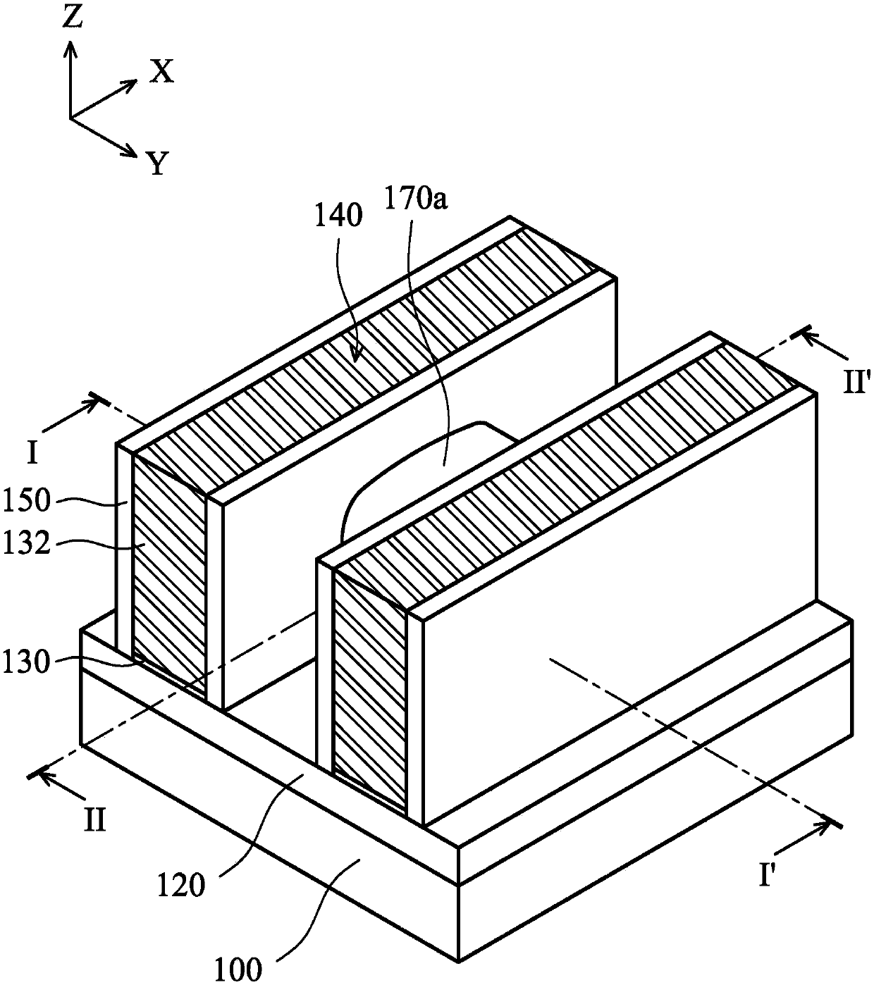
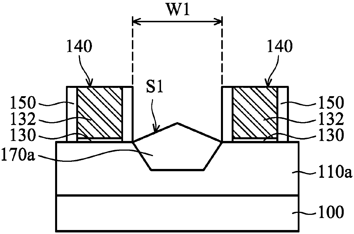
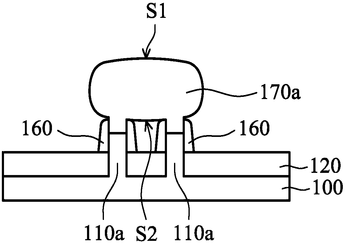
[0051] It is to be appreciated that the disclosure that follows this specification provides many different embodiments, or examples, for implementing the various features of the disclosure. However, the following disclosures in this specification describe specific examples of each component and its arrangement in order to simplify the description of the invention. Of course, these specific examples are not intended to limit the present disclosure. For example, if the following disclosure in this specification describes that a first characteristic component is formed on or above a second characteristic component, it means that it includes that the above-mentioned first characteristic component and the above-mentioned second characteristic component are formed directly Embodiments that are in contact also include embodiments where an additional feature is formed between the first feature and the second feature such that the first feature and the second feature may not be in dire...
PUM
 Abstract
Description
Claims
Application Information
 - R&D
- Intellectual Property
- Life Sciences
- Materials
- Tech Scout
- Unparalleled Data Quality
- Higher Quality Content
- 60% Fewer Hallucinations
Browse by: Latest US Patents, China's latest patents, Technical Efficacy Thesaurus, Application Domain, Technology Topic, Popular Technical Reports.
© 2025 PatSnap. All rights reserved.Legal|Privacy policy|Modern Slavery Act Transparency Statement|Sitemap|About US| Contact US: help@patsnap.com