Light emitting diode display

A light-emitting diode and display technology, applied in the field of display, to achieve the best display quality effect

Pending Publication Date: 2019-05-07
PLAYNITRIDE
View PDF6 Cites 3 Cited by
  • Summary
  • Abstract
  • Description
  • Claims
  • Application Information

AI Technical Summary

Problems solved by technology

The display cells are arranged in an array and connected to each other

Method used


Image

  • Light emitting diode display
  • Light emitting diode display
  • Light emitting diode display

Examples


Embodiment Construction

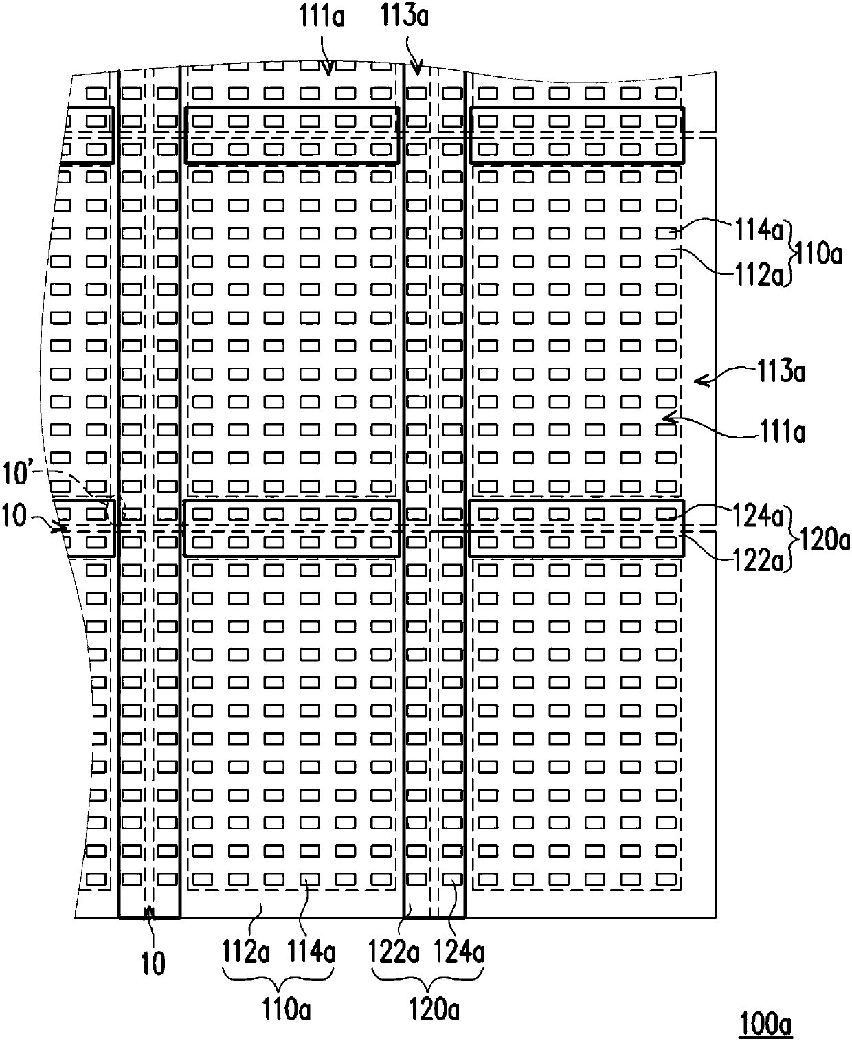
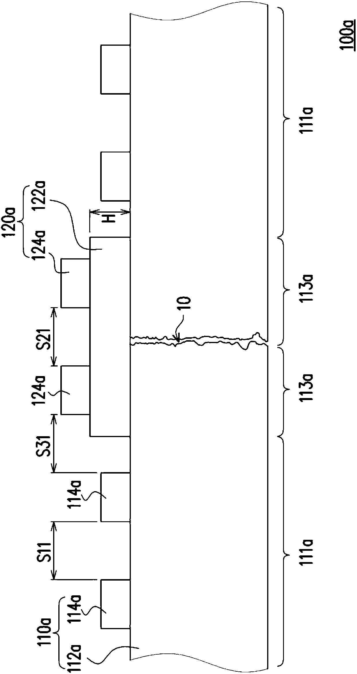
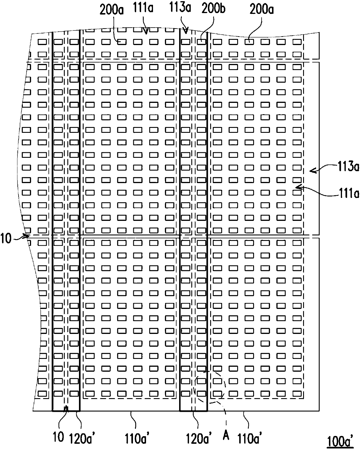
[0053] Figure 1A It is a schematic partial top view of a light emitting diode display according to an embodiment of the present invention. Figure 1B for Figure 1A A partial cross-sectional schematic of a light-emitting diode display. Please also refer to Figure 1A and Figure 1B , in this embodiment, the LED display 100a includes a plurality of display units 110a and a plurality of auxiliary display units 120a. The display units 110a are arranged in an array and connected to each other. Each display unit 110a has an element arrangement area 111a, a peripheral area 113a surrounding the element arrangement area 111a, and a plurality of first light emitting elements 114a disposed in the element arrangement area 111a and arranged in an array. The auxiliary display unit 120a is disposed on the peripheral area 113a of any two adjacent display units 110a. Each auxiliary display unit 120a includes an auxiliary substrate 122a and a plurality of second light emitting elements 124...


PUM


Abstract

A light emitting diode display includes a plurality of display units and a plurality of auxiliary display units. The display units are arranged in an array and connected with one another. Each displayunit has a component configuration area, a peripheral area around the component configuration area, and a plurality of first light emitting elements configured in the component configuration area andarranged in an array. Each auxiliary display unit is configured on the peripheral areas of any two adjacent display units. Each auxiliary display unit includes an auxiliary substrate and a pluralityof second light emitting elements arranged in an array. The second light emitting elements are arranged on the auxiliary substrates and are at a horizontal height different from that of the first light emitting elements. Each auxiliary substrate bridges two adjacent display units.

Description

technical field [0001] The invention relates to a display, in particular to a light-emitting diode display using light-emitting diodes as display pixels. Background technique [0002] In recent years, in order to maximize the screen size, display panels with narrow borders are more and more widely used in various devices. In order to realize large-size displays, the concept and application of splicing multiple display panels has gradually emerged. However, when multiple display panels are spliced ​​to form a large display, the frame width of the display panels often causes discontinuity in the display image at the junction between any two adjacent display panels. In addition, due to the relationship between the fineness of the manufacturing process on the side of each display panel, there will still be gaps at the joint at the microscopic level, and under the current trend of miniaturization of light-emitting diode elements (such as the size below 100 microns), it is easy t...

Claims


Application Information

Patent Timeline
Patent Type & Authority Applications(China)
IPC IPC(8): H01L27/15G09F9/33
Inventor 李允立林子旸陈培欣
Owner PLAYNITRIDE
Why Eureka
Try Eureka