Circuit board, semi-finished product and preparation method thereof, and electronic device

A technology for electronic devices and circuit boards, which is used in printed circuit manufacturing, printed circuits, printed circuit components, etc., can solve the problem of easy penetration of molding materials into circuit board units and lower molds, etc., to facilitate transportation and improve utilization. , the effect of improving reliability

Pending Publication Date: 2019-05-07
NINGBO SUNNY OPOTECH CO LTD
View PDF0 Cites 0 Cited by
  • Summary
  • Abstract
  • Description
  • Claims
  • Application Information

AI Technical Summary

Problems solved by technology

[0009] One object of the present invention is to provide a circuit board and its preparation method, which solves the problem that the molding material easily seeps between the circuit board unit and the lower mold when the circuit board is molded in the prior art

Method used


Image

  • Circuit board, semi-finished product and preparation method thereof, and electronic device
  • Circuit board, semi-finished product and preparation method thereof, and electronic device
  • Circuit board, semi-finished product and preparation method thereof, and electronic device

Examples


Embodiment approach

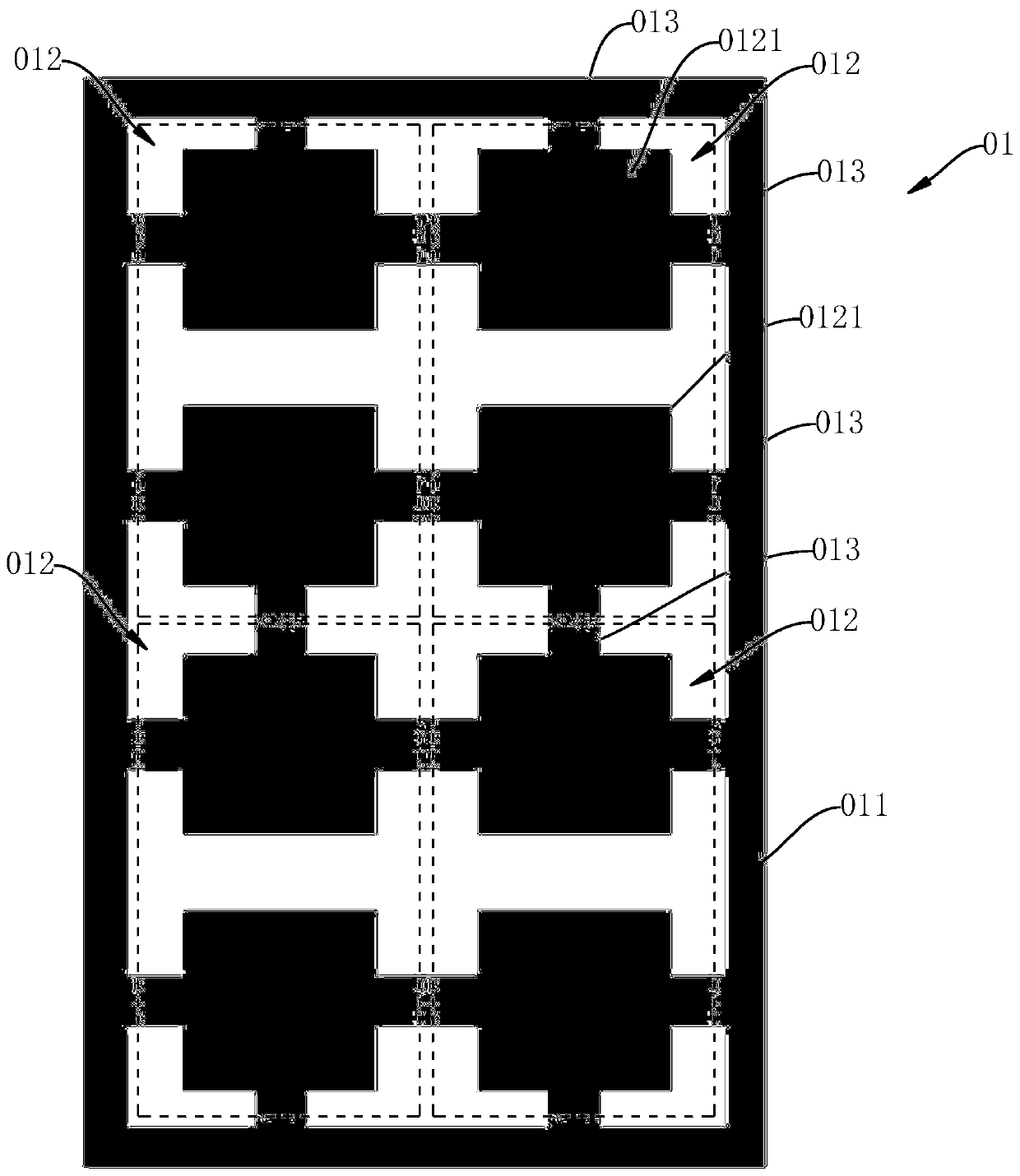
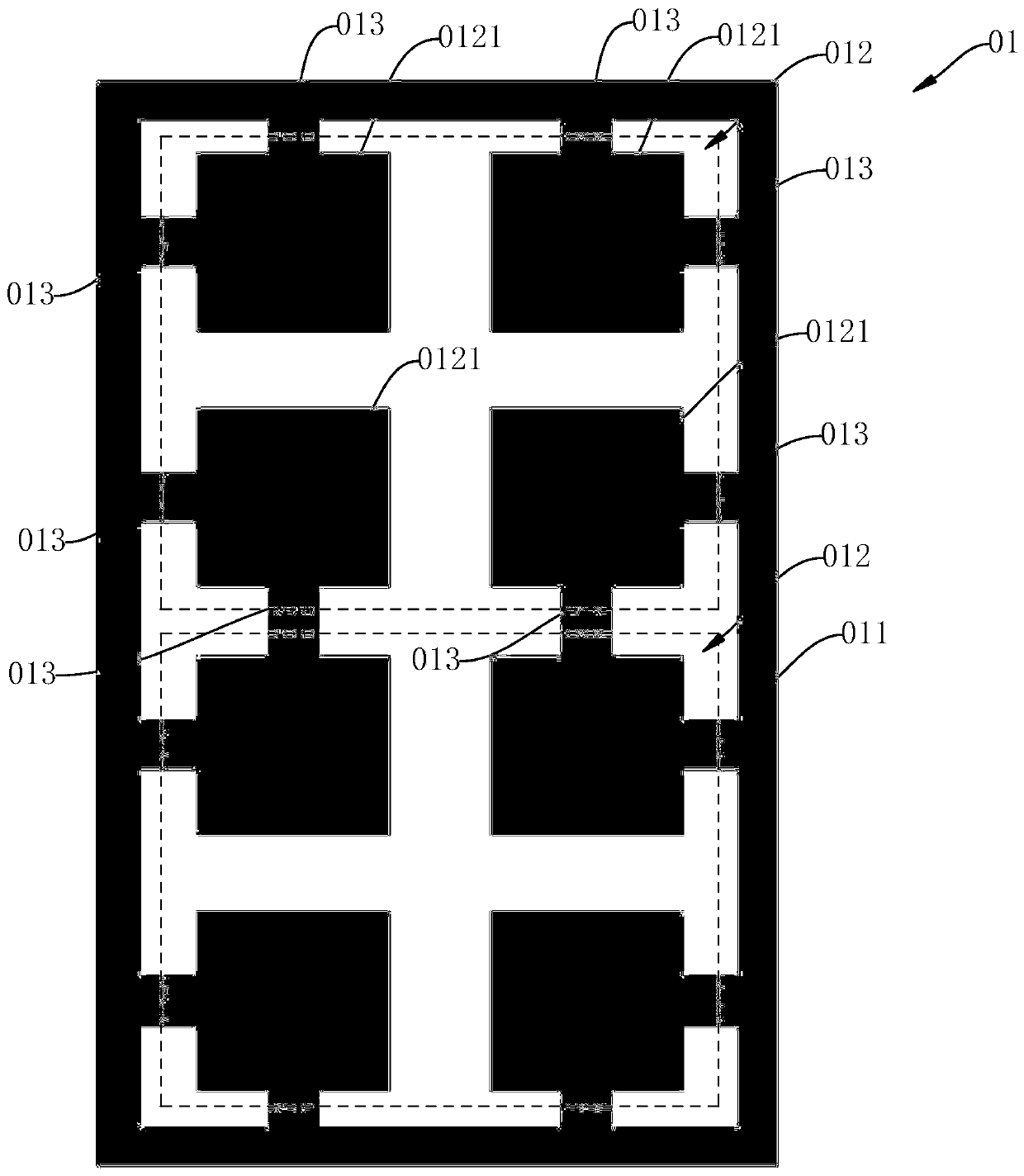
[0090] In some embodiments, the molded circuit board 3b includes a plurality of molded sub-circuit boards 31b and molding materials filled between the molded sub-circuit boards 31b, such as Figure 10C Or 10D or 10G. The circuit board unit 111 arranged on the molded circuit board 3b can fully overlap or partially overlap with the molded board sub-circuit board 31b, so that the circuit board unit 111 is conductively connected with the molded board sub-circuit board 31b, as Figure 10Cor 10D. Of course, the circuit board unit 111 arranged on the molded circuit board 3b can also not overlap with the molded sub-circuit board 31b, that is, the circuit board unit 111 is arranged on the surface formed by the molding material, such as Figure 10G As shown, at this time, the circuit board unit 111 and the molded board sub-circuit board 31b can choose whether to conduct a conductive connection according to actual needs, and if a conductive connection is required, the two can be connect...


PUM


Abstract

The invention discloses a circuit board, a semi-finished product and preparation method thereof and an electronic device. The circuit board comprises a substrate and circuit board units arranged on the substrate separate from each other, at least part of the first surface of each circuit board unit is combined with the surface of the substrate, the second surface of each circuit board unit is protruded out of the surface of the substrate, and the substrate includes a molding layer or a molding circuit board. The circuit board is prepared by molding and then etching, so that the finally formedcircuit board units are protruded out of the substrate. The circuit board units can maintain connection with the frame needless of a connecting part, and thus, the circuit board units are arranged more flexibly, and the material utilization rate of the etching layer is improved; and in addition, the circuit board units are flatter and tend not to warp.

Description

technical field [0001] The invention relates to the technical field of circuit board production, in particular to a circuit board, a semi-finished circuit board, an electronic device and a circuit board preparation method. Background technique [0002] The circuit board is a very important component in the camera module. In order to reduce the size of the camera module and improve the flatness of the base of the camera module, it is an existing method to mold the surface of the circuit board to obtain a flat mounting surface. practice. In order to improve the processing efficiency of circuit boards, several circuit boards or electrodes that need to be separated are usually integrally molded, and the preparation process usually includes the following steps [0003] Etching: Etching an etching board to obtain circuit board puzzle 01, such as figure 1 , 2 As shown, the circuit board assembly 01 includes an outer frame 011 and a plurality of circuit boards 012 arranged in the...

Claims


Application Information

Patent Timeline
Patent Type & Authority Applications(China)
IPC IPC(8): H05K1/14H05K3/00H05K1/18
Inventor 黄桢赵波杰
Owner NINGBO SUNNY OPOTECH CO LTD
Why Eureka
Try Eureka