Optical filter, and camera module and electronic device comprising the same

A technology of optical filters and organic dyes, which can be applied in the fields of optical filters, cameras, chemical instruments and methods for photographic purposes, and can solve the problems of few filters and so on.

Active Publication Date: 2019-05-14
SAMSUNG ELECTRONICS CO LTD
View PDF17 Cites 2 Cited by
  • Summary
  • Abstract
  • Description
  • Claims
  • Application Information

AI Technical Summary

Problems solved by technology

[0008] The above plastic substrate may contribute little to thinning the filter, but causes a glare phenomenon in which when an object with high brightness is observed or imaged, a border around the object is seen (wifi type glare phenomenon) , light spreading or flickering around the object (petal glare phenomenon), etc.

Method used


Image

  • Optical filter, and camera module and electronic device comprising the same
  • Optical filter, and camera module and electronic device comprising the same
  • Optical filter, and camera module and electronic device comprising the same

Examples


Embodiment 1

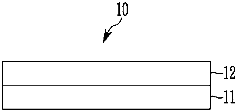
[0261] The first near-infrared absorbing layer was formed by coating a copper phosphate composition prepared by mixing a THF solvent and a copper phosphate represented by Chemical Formula 4a on a polymer film TAC film (Fuji Tekko Co., Ltd.) on and dry it.

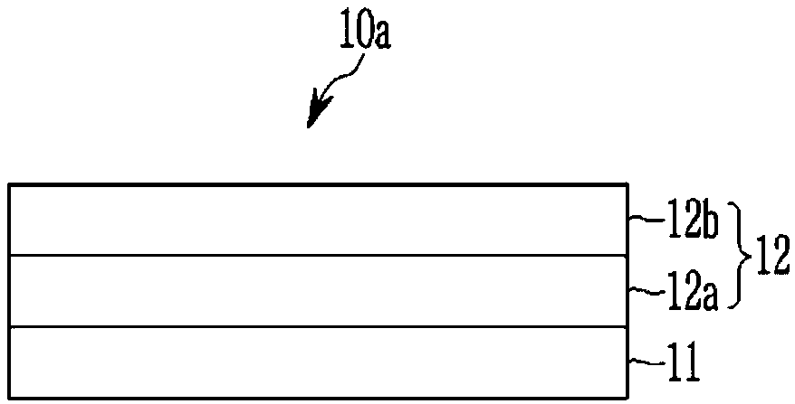
[0262] Subsequently, on the first near-infrared absorbing layer, a second near-infrared absorbing layer is formed by coating an organic dye represented by Chemical Formula 1a, an organic dye represented by Chemical Formula 2a, an acryl-based adhesive, A composition for the second near-infrared absorbing layer prepared by mixing with methyl ethyl ketone as an organic solvent, and then drying it.

[0263] On the second near-infrared absorbing layer, an anti-reflection coating (ARC-100, Don Co., Ltd.) was formed to manufacture an optical filter according to Example 1 (polymer film / first near-infrared absorbing layer / second near-infrared absorbing layer / anti-reflection layer). The filter has a thickness of about 120 μm.

Embodiment 2

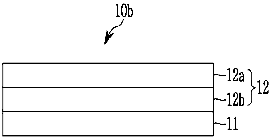
[0265] The optical filter (antireflection layer / polymer film / first near-infrared absorbing layer / second near-infrared absorbing layer / antireflection layer) according to Example 2 was manufactured according to the same method as in Example 1, except as follows: A polymer film having an antireflection layer (DSG-17TG60, Dai Nippon Printing Co., Ltd.) on the lower surface was used. The filter has a thickness of about 117 μm.

Embodiment 3

[0267] The optical filter (antireflection layer / polymer film / first near-infrared absorbing layer / second near-infrared absorbing layer / antireflection layer) according to Example 3 was manufactured according to the same method as in Example 1, except as follows: A polymer film having an anti-reflection layer (DSG-17TG60, Dai Nippon Printing Co., Ltd.) on the lower surface was used and an organic dye represented by Chemical Formula 3 was further included in the composition for the second near-infrared absorbing layer. The filter has a thickness of about 117 μm.


PUM

PropertyMeasurementUnit
thicknessaaaaaaaaaa
thicknessaaaaaaaaaa
thicknessaaaaaaaaaa

Abstract

An optical filter, and a camera module and an electronic device comprising the same are disclosed. The optical filter comprises a near infrared absorption layer on a polymer film. The polymer film hasa* of about -5.0 to about +5.0 and b* of about -5.0 to about +5.0 in a color coordinate expressed by a CIE Lab color space. The near infrared absorption layer may be configured to transmit light in avisible region and to selectively absorb at least one part of light in a near infrared region. The near infrared absorption layer includes a first near infrared absorption material including a copperphosphate ester compound and a second near infrared absorption material including at least two different organic dyes. The second near infrared absorption material has a maximum absorption wavelength(lambda max) in a wavelength region of about 650 nm to about 1200 nm.

Description

[0001] Cross References to Related Applications [0002] This application claims priority and benefit from Korean Patent Application No. 10-2017-0144897 filed with the Korean Intellectual Property Office on November 1, 2017, the entire contents of which are incorporated herein by reference. technical field [0003] Optical filters (optical filters) and camera modules and electronic devices including the same are disclosed. Background technique [0004] Recently, electronic devices such as mobile phones, digital cameras, camcorders, and cameras (cameras) including image sensors that store images as electrical signals have been widely used. [0005] The electronic device may include a filter having near-infrared absorption capability to reduce or prevent generation of optical distortion (distortion) caused by light in a region other than the visible region. [0006] The filter is generally installed in front of the image sensor of the camera module and thus functions to effec...

Claims


Application Information

Patent Timeline
Patent Type & Authority Applications(China)
IPC IPC(8): G02B5/22G03B11/00
CPCG02B5/223G02B5/208G02B1/04G02B1/11C08K5/0041C08K5/3417C08K5/29C08K5/521C08J7/04C08K2003/085C08K5/52C08K3/08C08K5/235C09B23/08C09B57/007C09B57/00C09B53/02H10K30/80H10K39/32
Inventor 元钟勋金畅基金炯俊李龙柱郑明燮
Owner SAMSUNG ELECTRONICS CO LTD
Why Eureka
Try Eureka