A method for growing light-emitting diode epitaxial wafers

A technology for light emitting diodes and a growth method, which is applied to the growth field of light emitting diode epitaxial wafers, can solve the problems of affecting the service life of LEDs, reducing the carrier recombination efficiency, and high defect density, achieving good crystal quality and flatness, and improving mechanical toughness. The effect of improving the degree of density and density and growth quality

Active Publication Date: 2020-08-14
HC SEMITEK ZHEJIANG CO LTD
View PDF7 Cites 0 Cited by
  • Summary
  • Abstract
  • Description
  • Claims
  • Application Information

AI Technical Summary

Problems solved by technology

[0006] The embodiment of the present invention provides a method for growing light-emitting diode epitaxial wafers, which can solve the problems of high line defect density, lower carrier recombination efficiency, lead to LED leakage and affect the service life of LED in the prior art

Method used


Image

  • A method for growing light-emitting diode epitaxial wafers

Examples


Embodiment Construction

[0028] In order to make the object, technical solution and advantages of the present invention clearer, the implementation manner of the present invention will be further described in detail below in conjunction with the accompanying drawings.

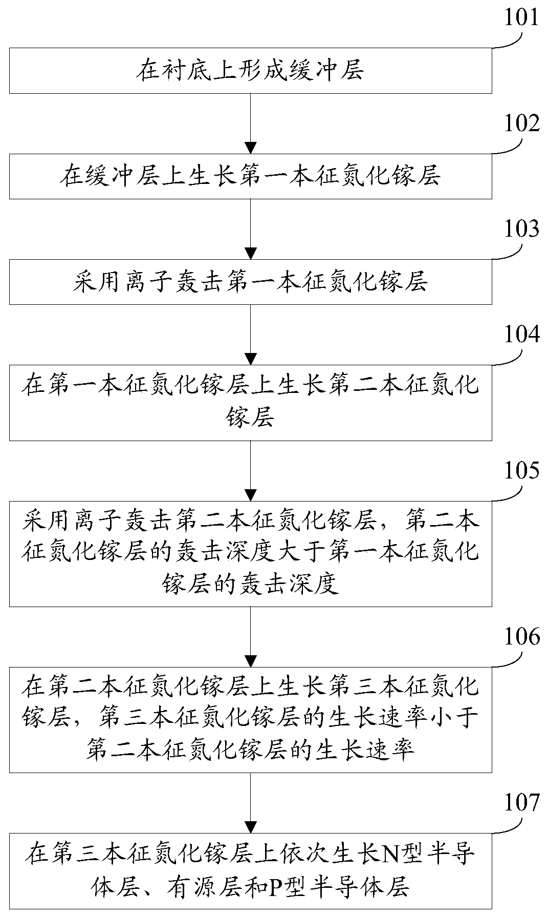
[0029] An embodiment of the present invention provides a method for growing an epitaxial wafer of a light emitting diode. figure 1 It is a flowchart of a method for growing a light-emitting diode epitaxial wafer provided by an embodiment of the present invention. see figure 1 , the growth method includes:

[0030] Step 101: forming a buffer layer on the substrate.

[0031] Specifically, the main role of the substrate is to provide a substrate for the growth of epitaxial materials. The substrate can be sapphire (the main component is Al 2 o 3 ) substrate, preferably a patterned sapphire substrate (English: Patterned Sapphire Substrate, PSS for short). Furthermore, the graphics in the PSS can be hemispherical, the diameter of the h...


PUM

PropertyMeasurementUnit
angle of incidenceaaaaaaaaaa
thicknessaaaaaaaaaa
thicknessaaaaaaaaaa

Abstract

The invention provides a growth method of a luminous diode epitaxial wafer, and belongs to the technical field of semiconductors. The growth method includes the steps that a buffer layer is formed ona substrate; a first intrinsic gallium nitride layer grows on the buffer layer; ions are used for bombarding the first intrinsic gallium nitride layer; a second intrinsic gallium nitride layer grows on the first intrinsic gallium nitride layer; ions are used for bombarding the second intrinsic gallium nitride layer, and the bombarding depth of the second intrinsic gallium nitride layer is larger than the bombarding depth of the first intrinsic gallium nitride layer; a third intrinsic gallium nitride layer grows on the second intrinsic gallium nitride layer, and the growth rate of the third intrinsic gallium nitride layer is lower than the growth rate of the second intrinsic gallium nitride; and an N type semiconductor layer, an active layer and a P type semiconductor layer sequentially grow on the third intrinsic gallium nitride layer. According to the growth method of the luminous diode epitaxial wafer, the density of internal wiring defects of the epitaxial wafer can be effectively reduced.

Description

technical field [0001] The invention relates to the technical field of semiconductors, in particular to a method for growing a light-emitting diode epitaxial wafer. Background technique [0002] Light Emitting Diode (English: Light Emitting Diode, referred to as: LED) as a new generation of high-efficiency and green solid-state lighting sources, since the gallium nitride (GaN)-based LED was successfully developed by Japanese scientists in the 1990s, its technology has continued to improve , the luminous brightness is continuously improved, and the application fields are becoming wider and wider. LED has the advantages of low voltage, low power consumption, small size, light weight, long life, high reliability, etc., and is being rapidly and widely used in display screens and other fields. Especially for GaN-based LEDs, since GaN-based materials are semiconductor materials with a wide bandgap (about 3.4eV), they can meet the conditions for generating blue light with high pho...

Claims


Application Information

Patent Timeline
Patent Type & Authority Patents(China)
IPC IPC(8): H01L33/00
Inventor 兰叶顾小云
Owner HC SEMITEK ZHEJIANG CO LTD
Why Eureka
Try Eureka