
A kind of circuit board and using method thereof

A technology of circuit boards and substrates, which is applied in the direction of printed circuit components, etc., can solve the problems of increased difficulty in current testing, irreparability, thin trace width, etc., and achieve the effects of improving measurement convenience, simple design, and clear principles

Active Publication Date: 2020-05-15
BOE TECH GRP CO LTD +1
View PDF4 Cites 0 Cited by
  • Summary
  • Abstract
  • Description
  • Claims
  • Application Information

AI Technical Summary

Problems solved by technology

When testing the current, it is necessary to connect the measuring device in series to the circuit, and most of the existing electronic equipment uses a circuit board to design a circuit or uses a connector (such as the connection between the mobile phone module screen and the main board through a circuit connector) to Different modules are electrically connected, which requires the circuit board to be cut off from the access point of the welding measurement device. However, due to the relatively dense wiring of electronic equipment and the relatively thin wiring width, it is easy to cut off adjacent lines or other underlying lines, resulting in circuit failure. Cases where the board is damaged beyond repair, and manual soldering of measuring devices can also complicate current testing

Method used


Image

  • A kind of circuit board and using method thereof
  • A kind of circuit board and using method thereof
  • A kind of circuit board and using method thereof

Examples


Embodiment Construction

[0058] In order to illustrate the present invention more clearly, the present invention will be further described below in conjunction with preferred embodiments and accompanying drawings. Similar parts in the figures are denoted by the same reference numerals. Those skilled in the art should understand that the content specifically described below is illustrative rather than restrictive, and should not limit the protection scope of the present invention.

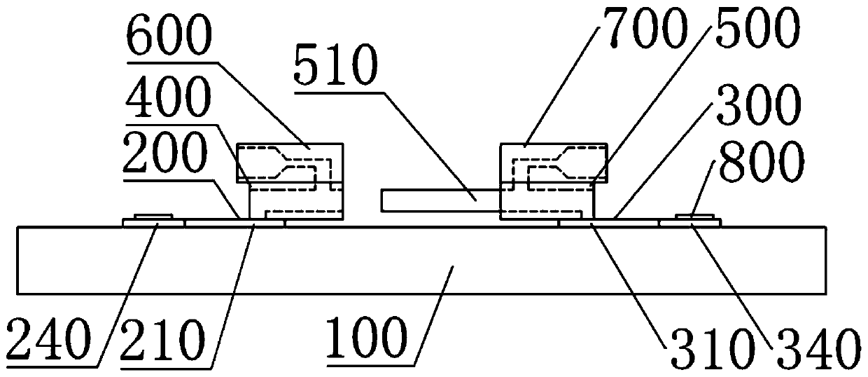
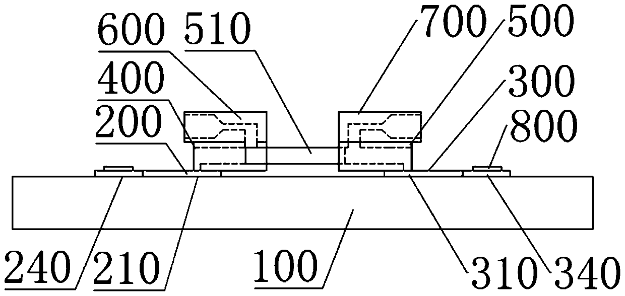
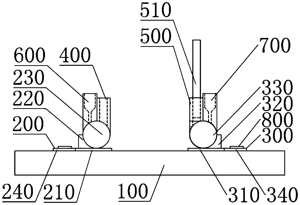
[0059] figure 1 It shows a schematic structural diagram of a circuit board proposed by an embodiment of the present invention, such as figure 1 As shown, the circuit board includes a substrate 100 and a first conductive layer 200 and a second conductive layer 300 oppositely arranged on the substrate 100, the first conductive layer 200 and the second conductive layer 300 are electrically insulated from each other, wherein the first to be The test pin and the second pin to be tested are electrically connected to the first ...


PUM


Abstract

The invention discloses a circuit board. The circuit board comprises a substrate, a first conductive layer, a second conductive layer, a first electric connector, a second electric connector, a thirdelectric connector and a fourth electric connector; the first conductive layer and the second conductive layer are electrically insulated with each other; the outside surface of the first electric connector is insulated; a first metal layer is formed on the inside surface of the first electric connector; the first conductive layer is electrically connected with the first metal layer; the outside surface of the second electric connector is insulated; a second metal layer is formed on the inside surface of the second electric connector; the second conductive layer is electrically connected withthe second metal layer; the second electric connector comprises a metal column structure, which can extend out of a second opening end; the outside surface of the third electric connector is insulated; a third metal layer is formed on the inside surface of the third electric connector; the first metal layer is electrically connected with the third metal layer; the outside surface of the fourth electric connector is insulated; a fourth metal layer is formed on the inside surface of the fourth electric connector; and the second metal layer is electrically connected with the fourth metal layer. By means of the circuit board in the invention, a circuit can be tested while a primary circuit is not damaged and a welding measurement device is not required.

Description

technical field [0001] The invention relates to the technical field of circuit testing, in particular to a circuit board and a method for using the same. Background technique [0002] Currently, electronic equipment usually uses a measuring device such as a multimeter to measure current data in various circuits to check whether the electrical parameters are correct. When testing the current, it is necessary to connect the measuring device in series to the circuit, and most of the existing electronic devices use circuit boards to design circuits or use connectors (such as the connection between the mobile phone module screen and the main board through circuit connectors) to Different modules are electrically connected, which requires the circuit board to be cut off from the access point of the welding measurement device. However, due to the relatively dense wiring of electronic equipment and the relatively thin width of the wiring, it is easy to cut off adjacent lines or othe...

Claims


Application Information

Patent Timeline
Patent Type & Authority Patents(China)
IPC IPC(8): H05K1/02
Inventor 王国春吴昊刘旭忠安娜次刚马晓宫心峰张铮许少鹏徐斌罗振华管清竹于作鑫刘殿中宗正董鹏程
Owner BOE TECH GRP CO LTD
Learn More