

a display panel
A display panel and display area technology, which is applied to semiconductor devices, electrical components, circuits, etc., can solve the problems of aging and failure of light-emitting materials of organic light-emitting units, affecting the life of display panels, etc.
- Summary
- Abstract
- Description
- Claims
- Application Information
AI Technical Summary
Problems solved by technology
Method used
Image

Examples
Embodiment Construction
[0035] The present invention will be further described in detail below in conjunction with the accompanying drawings and embodiments. It should be understood that the specific embodiments described here are only used to explain the present invention, but not to limit the present invention. In addition, it should be noted that, for the convenience of description, only some structures related to the present invention are shown in the drawings but not all structures.
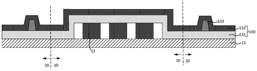
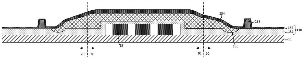
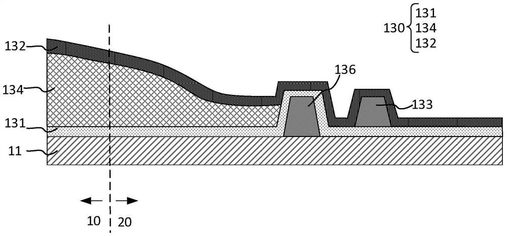
[0036] figure 1 A schematic cross-sectional structure diagram of a display panel provided by an embodiment of the present invention, as shown in figure 1 As shown, the display panel includes a substrate 11 , an organic light emitting unit 12 and a thin film encapsulation layer 130 . The substrate 11 includes a display area 10 and a non-display area 20 , the organic light emitting unit 12 is disposed on the display area 10 of the substrate 11 , and the thin film encapsulation layer 130 covers the organic light emi...
PUM
 Abstract
Description
Claims
Application Information