Pressing structure for correcting warping of plastic package flat plate and semiconductor device

A semiconductor and flat-panel technology, used in semiconductor/solid-state device manufacturing, electrical components, circuits, etc., can solve problems such as adverse effects, impact on service life or performance, and achieve the effect of ensuring thermal insulation

Inactive Publication Date: 2019-05-28
NAT CENT FOR ADVANCED PACKAGING
View PDF3 Cites 2 Cited by
  • Summary
  • Abstract
  • Description
  • Claims
  • Application Information

AI Technical Summary

Problems solved by technology

[0004] Therefore, the technical problem to be solved by the present invention is to overcome the problem that the device used to correct the warped plastic package in the prior art is easy to transfer heat to other structures when the plastic package is heated, causing adverse effects on these structures, thereby affecting Technical defects su...

Method used


Image

  • Pressing structure for correcting warping of plastic package flat plate and semiconductor device
  • Pressing structure for correcting warping of plastic package flat plate and semiconductor device
  • Pressing structure for correcting warping of plastic package flat plate and semiconductor device

Examples


Embodiment 1

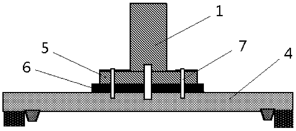
[0034] Such as figure 1 As shown in -2, the present invention provides a pressing structure for correcting warpage of a plastic-encapsulated flat panel semiconductor device, which includes a pressing platform 4, a connection structure and a heat insulation structure.

[0035] In this embodiment, the pressing platform 4 moves back and forth along the direction perpendicular to the plastic-encapsulated flat panel, and is used to apply pressure to the plastic-encapsulated flat panel 9 located below. The pressing end where the above-mentioned plastic sealing flat plate 9 contacts, the pressing platform 4 can be driven by electric, pneumatic or oil pressure to move.

[0036] In this embodiment, one end of the connecting structure is connected to the pressing platform 4, and the other end is connected to a driving device for driving the pressing platform 4 to and fro, and the connecting structure is arranged on the side of the pressing platform 4. Above, in order to apply pressure ...

Embodiment 2

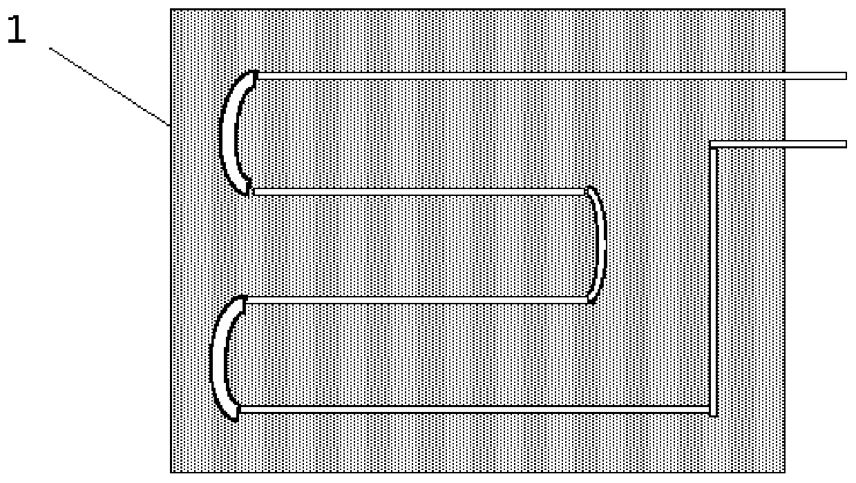
[0045] Such as image 3 As shown, the connecting structure includes a connecting rod 1 and a joint 3 connected to the connecting rod 1 and the pressing platform 4 respectively. The difference from Example 1 is that the heat insulation structure is arranged on the joint 3 Several holes in the interior 2. The joint 3 is made of low heat conduction material. In this embodiment, the joint 3 is made of stainless steel, and a plurality of small cavities are processed inside the joint 3, which can reduce heat conduction, so that the heat transmitted through the joint to other structures A small amount of heat will not affect other structures. Further, the joint 3 is screwed to the pressing platform 4 and the connecting rod 1 .

Embodiment 3

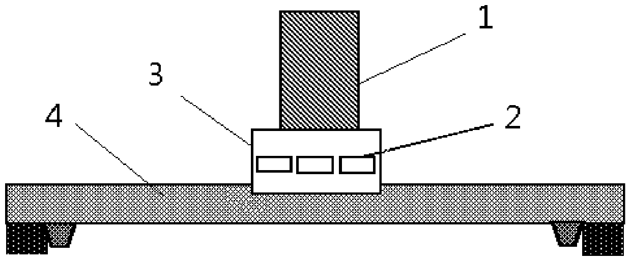
[0047] Such as Figure 4 As shown, this embodiment provides a semiconductor device for correcting a warped plastic-encapsulated flat panel, including the pressing structure described in Embodiment 1 and Embodiment 2, and further comprising The carrying platform 8 of the flat plate 9, the second heating device is arranged on the said carrying platform 8, the design of the first heating device and the second heating device can heat it from the upper surface and the lower surface of the plastic sealing flat plate respectively, so that the plastic sealing The heating effect of the flat plate is better.

[0048] In this embodiment, a support frame 10 is also provided below the carrying platform 8 to provide highly stable and flat surface support for the carrying platform 8. key structure.


PUM


Abstract

The invention relates to the technical field of plastic package flat plate correction, in particular to a pressing structure of a semiconductor device for correcting the warping of a plastic package flat plate and the semiconductor device. The pressing structure comprises a pressing platform which moves back and forth in the direction perpendicular to the plastic packaging flat plate and is used for applying pressure to the plastic packaging flat plate arranged below; and a connection structure, wherein one end of the connecting structure is connected with the pressing platform, the other endof the connecting structure is connected with a driving device used for driving the pressing platform to move back and forth, and a heat insulation structure used for preventing heat in the pressing platform from being transmitted outwards from the pressing platform through the connecting structure is arranged between the connecting structure and the pressing platform. The semiconductor device comprises a pressing structure and a bearing platform arranged below the pressing structure and used for bearing a plastic package flat plate. According to the pressing structure of the semiconductor device for correcting the warping of the plastic package flat plate, when the plastic package flat plate is heated, heat can be prevented from being transferred into other structures through the heat insulation structure, and therefore the influence on other structures is reduced or eradicated.

Description

technical field [0001] The invention relates to the technical field of advanced packaging of integrated circuits, in particular to a pressing structure of a semiconductor device used to correct the warpage of a plastic-encapsulated flat plate and the semiconductor device. Background technique [0002] In the process of fan-out packaging, the large-size flat panel molded by plastic encapsulation and reconstruction often shows a large warpage after cooling to room temperature due to the difference in physical properties between the materials used. Since the follow-up process requires the surface of the chip reconstruction plate to be extremely flat, the warped plate will prevent other subsequent equipment from completing the high-quality process, resulting in defective packaging chips in the affected area on the plate. [0003] After many experiments, such as plastic packaging material selection, bare chip thickness optimization, plastic packaging process debugging, etc., the ...

Claims


Application Information

Patent Timeline
IPC IPC(8): H01L21/67
Inventor 姚大平
Owner NAT CENT FOR ADVANCED PACKAGING
Why Eureka
Try Eureka