Array substrate and manufacturing method of the array substrate

A technology for array substrates and substrates, applied in semiconductor/solid-state device manufacturing, electrical components, transistors, etc., can solve the problems of many interface defects between semiconductor layers and insulating layers, high cost, and large flat-band voltage drift

Inactive Publication Date: 2019-05-28
WUHAN CHINA STAR OPTOELECTRONICS SEMICON DISPLAY TECH CO LTD
View PDF6 Cites 0 Cited by
  • Summary
  • Abstract
  • Description
  • Claims
  • Application Information

AI Technical Summary

Problems solved by technology

[0003] Among them, due to N 2 The N element in O will cause more defects at the interface between the semiconductor layer and the insulating layer, resulting in large flat-band voltage drift, resulting in electrical instability of the product
Therefore, the industry mostly adopts TEOS / O 2 The way to form the insulating layer, but the cost of this way is higher

Method used


Image

  • Array substrate and manufacturing method of the array substrate
  • Array substrate and manufacturing method of the array substrate

Examples


Embodiment Construction

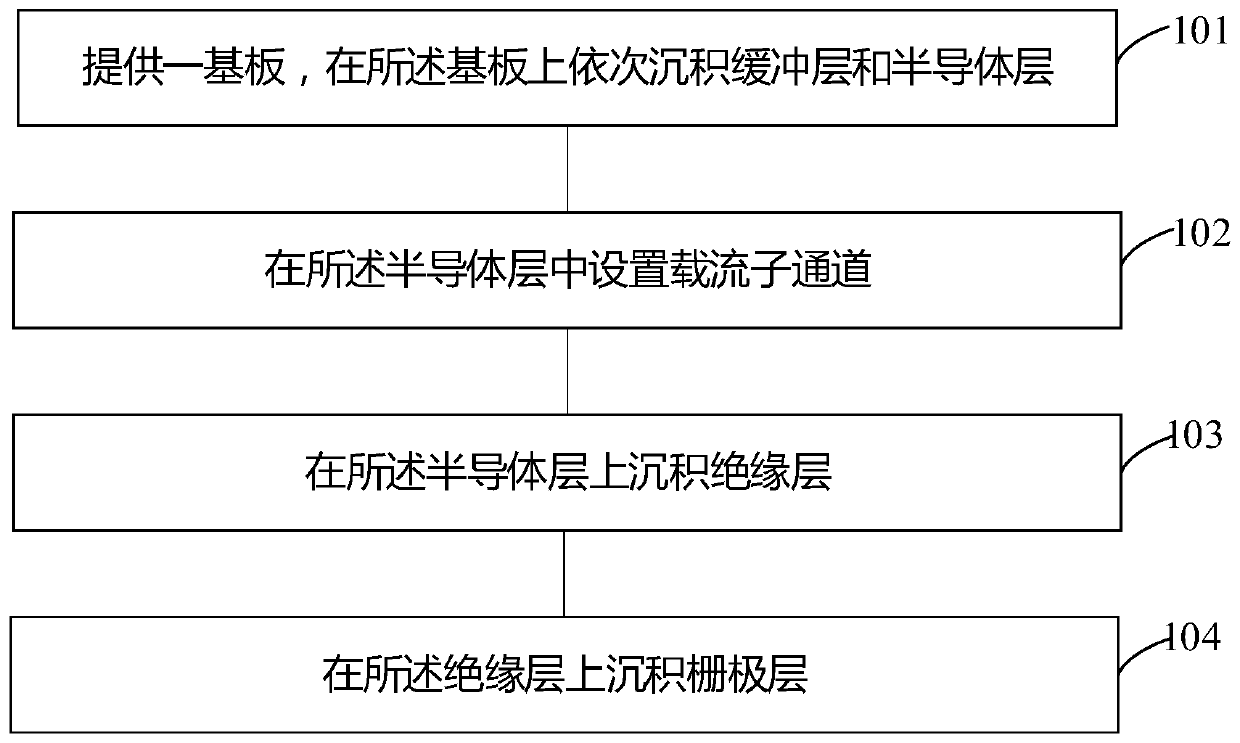
[0030] The technical solutions in the embodiments of the present application will be clearly and completely described below in conjunction with the drawings in the embodiments of the present application. Apparently, the described embodiments are only some of the embodiments of this application, not all of them. Based on the embodiments in this application, all other embodiments obtained by those skilled in the art without making creative efforts belong to the scope of protection of this application.

[0031] Embodiments of the present application provide an array substrate and a method for manufacturing the array substrate, which will be described in detail below.

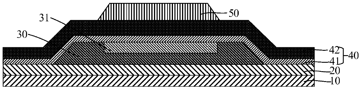
[0032] see figure 1 , figure 1 is a schematic structural diagram of the array substrate provided in the embodiment of the present application. The array substrate provided in the embodiment of the present application may include: a substrate 10 , a buffer layer 20 , a semiconductor layer 30 , an insulating layer...


PUM


Abstract

The embodiment of the invention discloses an array substrate and a manufacturing method of the array substrate. The array substrate comprises a substrate, a buffer layer, a semiconductor layer, an insulating layer and a grid layer. The buffer layer is arranged on the substrate; the semiconductor layer is arranged on the buffer layer; the insulating layer covers the buffer layer and the semiconductor layer; the grid electrode layer is arranged on the insulating layer; the semiconductor layer comprises a current carrier channel; the carrier channel is located on one side, facing the insulating layer, of the semiconductor layer; the insulating layer comprises a first thin film layer and a second thin film layer; the first thin film layer covers the semiconductor layer and the buffer layer; the second thin film layer covers the first thin film layer; the grid electrode layer is located on the second thin film layer; the density of the first thin film layer is larger than that of the secondthin film layer; and the carrier channel is connected with the first thin film layer. According to the scheme, the electrical stability of the array substrate can be improved.

Description

technical field [0001] The present application relates to the field of display technology, and in particular to an array substrate and a method for manufacturing the array substrate. Background technique [0002] In existing low temperature polysilicon technology (LTPS, Low Temperature Poly-silicon) products, the insulating layer between the semiconductor layer and the gate layer is often passed through TEOS / O 2 or SiH 4 / N 2 O is deposited in two ways. [0003] Among them, due to N 2 The N element in O will cause more defects at the interface between the semiconductor layer and the insulating layer, resulting in large flat-band voltage drift, resulting in electrical instability of the product. Therefore, the industry mostly adopts TEOS / O 2 The insulating layer is formed by a method, but the cost of this method is relatively high. Contents of the invention [0004] Embodiments of the present application provide an array substrate and a method for manufacturing the ar...

Claims


Application Information

Patent Timeline
Patent Type & Authority Applications(China)
IPC IPC(8): H01L29/786H01L29/423H01L21/336
CPCH01L29/423H01L29/4908H01L29/42384H01L29/78696H01L29/66757H01L29/78675H01L27/1248H01L27/1259
Inventor 谭威
Owner WUHAN CHINA STAR OPTOELECTRONICS SEMICON DISPLAY TECH CO LTD
Why Eureka
Try Eureka