Formation method of silicon oxide film and metal-insulator-metal capacitor

A silicon oxide and thin film technology, applied in metal material coating process, circuits, electrical components, etc., can solve the problems of poor dynamic characteristics of MIM capacitors, and achieve the effect of improving dynamic characteristics, stable electrical performance, and optimizing process conditions.

Active Publication Date: 2012-07-18
SEMICONDUCTOR MANUFACTURING INTERNATIONAL (BEIJING) CORP
View PDF1 Cites 0 Cited by
  • Summary
  • Abstract
  • Description
  • Claims
  • Application Information

AI Technical Summary

Problems solved by technology

[0009] The invention provides a method for forming a silicon oxide film and a metal-insulator-metal type capacitor to improve the poor dynamic characteristics of the existing MIM capacitor

Method used


Image

  • Formation method of silicon oxide film and metal-insulator-metal capacitor
  • Formation method of silicon oxide film and metal-insulator-metal capacitor
  • Formation method of silicon oxide film and metal-insulator-metal capacitor

Examples


no. 1 example

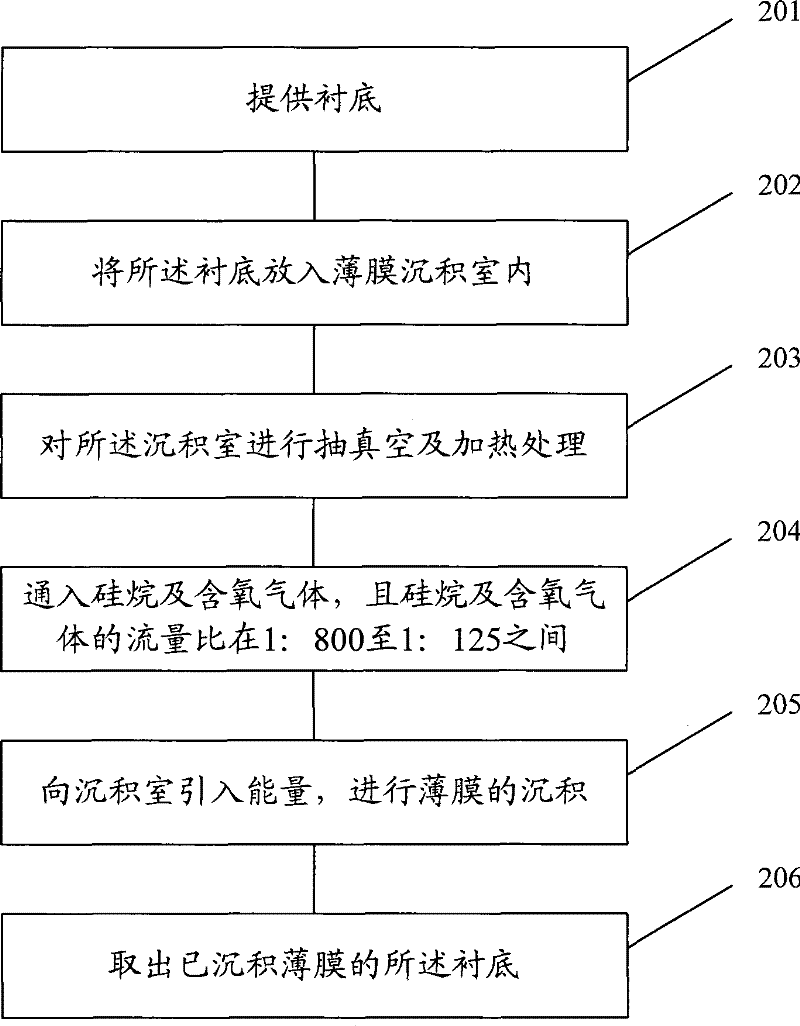
[0066] The first embodiment of the present invention introduces a new method for forming a silicon oxide film, figure 2 It is a flow chart of the method for forming a silicon oxide film in the first embodiment of the present invention, combined below figure 2 The first embodiment of the present invention will be described in detail.

[0067] Step 201: providing a substrate.

[0068] The substrate provided in this embodiment may be a simple silicon substrate, or a silicon substrate on which metal oxide semiconductor transistors have been formed, or a substrate on which an underlying metal wiring structure has been formed.

[0069] In other embodiments of the present invention, semiconductor substrates of other materials may also be used, such as germanium substrates, gallium arsenide substrates, and the like.

[0070] Step 202: Put the substrate into a film deposition chamber.

[0071] The film deposition equipment used in this embodiment is PECVD. In this step, the substr...

no. 2 example

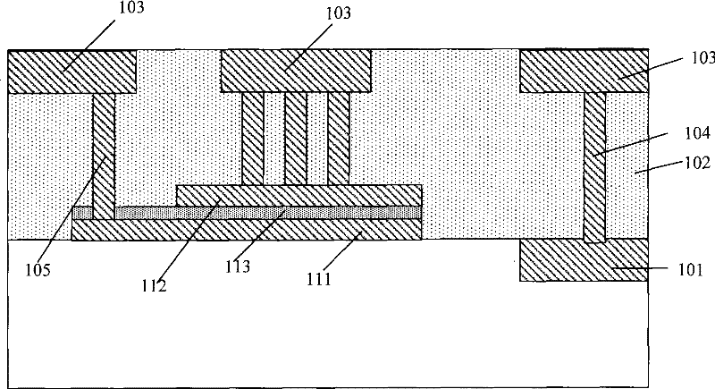
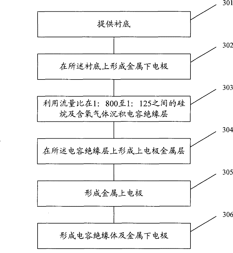
[0088] The second embodiment of the present invention introduces a new method for forming a MIM capacitor, image 3 It is a flowchart of a method for forming a MIM capacitor according to the second embodiment of the present invention, Figure 4 to Figure 10 In order to illustrate the schematic cross-sectional view of the device of the MIM capacitance forming method of the second embodiment of the present invention, the following is combined Figure 3 to Figure 10 The second embodiment of the present invention will be described in detail.

[0089] Step 301: Provide a substrate.

[0090] The substrate provided in this embodiment may be a silicon substrate on which a metal oxide semiconductor transistor has been formed, or a substrate on which an underlying metal wiring structure has been formed.

[0091] Figure 4 is a schematic cross-sectional view of the substrate provided in the second embodiment of the present invention, such as Figure 4 As shown, the underlying conduct...


PUM

PropertyMeasurementUnit
poweraaaaaaaaaa

Abstract

The invention discloses a formation method of a silicon oxide film, comprising the following steps of: providing a substrate, placing the substrate into a film deposition chamber, vacuumizing the deposition chamber, heating the deposition chamber, introducing silicane and oxygenous gas to the deposition chamber, wherein the flow ratio of silicane to oxygenous gas is between 1:800 and 1:125, introducing energy to the deposition chamber to deposit the film, and taking out the substrate with the deposited film. The invention also discloses a corresponding formation method of a metal-insulator-metal capacitor. The metal-insulator-metal capacitor formed by using the silicon oxide film method reduces and stabilizes a voltage coefficient of capacitance and a temperature coefficient of capacitance of the capacitor, improves the dynamic characteristics of the capacitor and enhances the electrical property stability of the capacitor.

Description

technical field [0001] The invention relates to the technical field of semiconductor manufacturing, in particular to a method for forming a silicon oxide film and a metal-insulator-metal (MIM) capacitor. Background technique [0002] The integrated circuit manufacturing process is a planar manufacturing process that combines photolithography, etching, deposition, ion implantation and other processes to form a large number of various types of complex devices on the same substrate and connect them to each other to have a complete electronic functions. Among them, capacitors are electronic components commonly used in integrated circuit technology, and can be widely used in circuits such as couplers, filters, and oscillators. [0003] Among existing integrated circuit capacitors, metal-insulator-metal (MIM, Metal-insulator-metal) capacitors have gradually become mainstream in radio frequency integrated circuits. The reason is that it is usually made in the metal interconnectio...

Claims


Application Information

Patent Timeline
Patent Type & Authority Patents(China)
IPC IPC(8): C23C16/40C23C16/455H01L21/316H01L21/02
Inventor 蔡明邹晓东徐强
Owner SEMICONDUCTOR MANUFACTURING INTERNATIONAL (BEIJING) CORP
Why Eureka
Try Eureka