The invention relates to a micron-scale ID image identification method and a micron-scale ID image identification system

An image recognition, micron-level technology, applied in the field of image recognition, can solve the problem of inability to accurately identify micron-level ID images on chips in large quantities, and achieve the effect of improving production efficiency, improving work efficiency and improving accuracy.

Active Publication Date: 2019-05-31
北京蓝骏创科信息技术有限公司
View PDF0 Cites 1 Cited by
  • Summary
  • Abstract
  • Description
  • Claims
  • Application Information

AI Technical Summary

Problems solved by technology

[0006] In view of the above problems, the object of the present invention is to overcome the defect that the micron-level ID image on the chip cannot be accurately and mass-identified in the prior art, and to provide a method and system for micron-level ID image recognition

Method used


Image

  • The invention relates to a micron-scale ID image identification method and a micron-scale ID image identification system
  • The invention relates to a micron-scale ID image identification method and a micron-scale ID image identification system
  • The invention relates to a micron-scale ID image identification method and a micron-scale ID image identification system

Examples


Embodiment approach

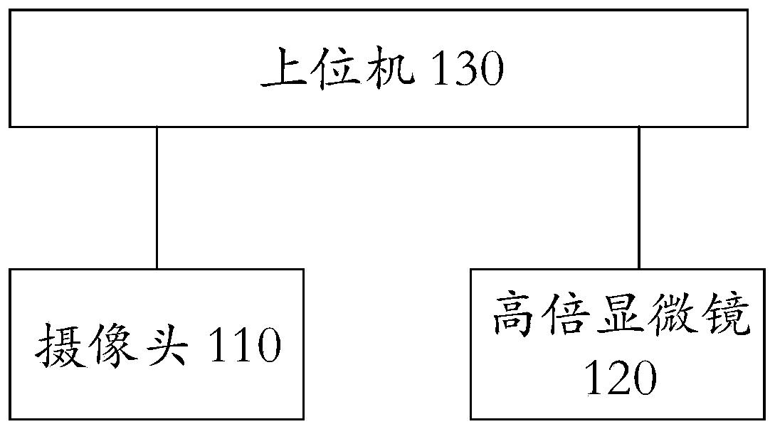
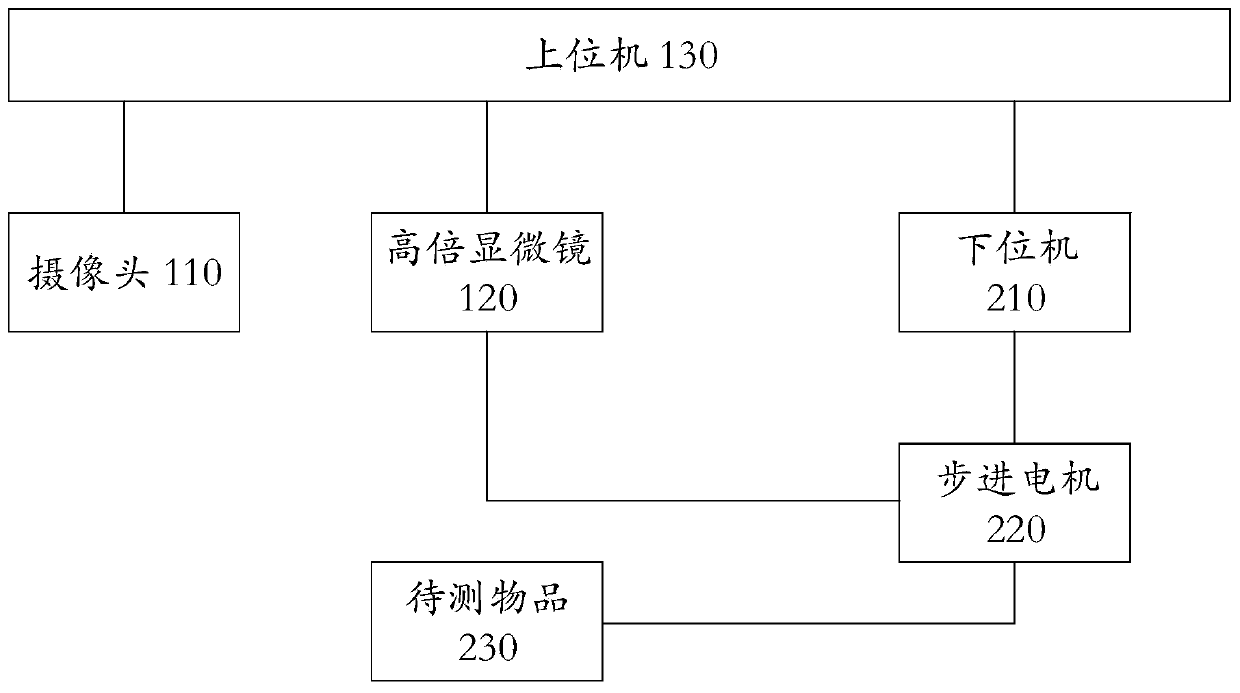
[0062] According to an embodiment of the present invention, the positional relationship of the items to be tested may be placed according to a preset arrangement for easy identification. The preset arrangement means that it is designed in advance to arrange according to a certain rule or order. For example, the preset arrangement may include a 6×5 or 16×10 matrix, or other Arrangement forms, such as n×n squares, triangles, etc. For example, the items to be tested are placed in the packaging box, and are placed neatly according to the designed chip placement position in the packaging box, instead of being placed irregularly such as stacking each other.

[0063]The sequentially recording the corresponding ID information may be recorded in the same arrangement form as the positional relationship of the items to be tested. The ID information on the item to be tested is sequentially recorded according to the order in which the item to be tested is observed by the high-power micros...


PUM


Abstract

The invention provides a micron-scale ID image recognition method and system, and the method comprises the steps: observing the overall condition of a to-be-detected object, so as to determine the number and position relation S1 of the to-be-detected object, and enabling the number of the to-be-detected object to be one or more; And adjusting a view field, sequentially identifying the ID images ofthe to-be-detected object, and sequentially recording corresponding ID information S2. According to the technical scheme provided by the invention, the work of manually identifying and recording thechip ID with naked eyes by using a microscope can be replaced, automatic identification and recording are realized, the technical requirement on an operator is reduced, the accuracy of identificationand recording is greatly improved, and the working efficiency is improved; Through the secondary imaging positioning combined by the large-view-field camera and the high-power microscope, the problemthat automatic positioning cannot be achieved due to the fact that chip packaging boxes are different and ID positions are different is solved.

Description

technical field [0001] The present invention generally relates to the field of image recognition, and more specifically, relates to a micron-level ID image recognition technology. Background technique [0002] The ID number on the chip is relatively small in size, such as laser chips, even at the micron level, such as attached Figure 14 as shown, Figure 14 The size of a single number or letter in the ID number 5A is only a dozen microns, and even the ID number on some chips is only a few microns. All such IDs cannot be seen directly with the naked eye, and must be observed under a microscope with a magnification of 200~ 400 times. In actual work, it is often necessary to identify the ID numbers on the chips accurately and in large quantities. [0003] In the current practical work, the laser chip to be identified is usually placed on the stage of the microscope, and the field of view of the objective lens and the focal length of the microscope are adjusted so that the ID ...

Claims


Application Information

Patent Timeline
Patent Type & Authority Applications(China)
IPC IPC(8): G06K9/20G06K9/00H04N5/225G02B21/36
Inventor 程木海马潮聂嵩
Owner 北京蓝骏创科信息技术有限公司
Why Eureka
Try Eureka