Shape processing method for PTFE antenna PCB product without internal positioning narrow edges

A technology of shape processing and PTFE, which is applied in the field of PCB manufacturing, can solve the problems of small size that does not meet the cleaning requirements of finished product cleaning machines, difficult to clean oxides, and low efficiency, so as to meet mass production, ensure product quality, and eliminate The effect of being oversized or undersized

Active Publication Date: 2019-06-04
HUIZHOU KING BROTHER CIRCUIT TECH +2
View PDF4 Cites 0 Cited by
  • Summary
  • Abstract
  • Description
  • Claims
  • Application Information

AI Technical Summary

Problems solved by technology

[0002] 5G applications will gradually increase from 3GHz to 6GHz or even higher frequency of 30GHz to transmit high-speed signals, which will bring new technical challenges to the manufacture and processing of antenna radio frequency materials
Moreover, because the size of the formed ultra-narrow antenna PCB product is too small to meet the cleaning requirements of the finished product cleaning machine, it can only be wiped manually with alcohol, which is not only slow and inefficient, but also the oxides are not easy to clean.

Method used


Image

  • Shape processing method for PTFE antenna PCB product without internal positioning narrow edges
  • Shape processing method for PTFE antenna PCB product without internal positioning narrow edges
  • Shape processing method for PTFE antenna PCB product without internal positioning narrow edges

Examples


Embodiment Construction

[0025] It should be understood that the specific embodiments described here are only used to explain the present invention, not to limit the present invention.

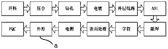
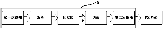
[0026] Such as Figure 1-2 As shown in , the shape processing method a of a narrow-side antenna PCB provided by an embodiment of the present invention can be applied to the existing manufacturing process of a narrow-side antenna PCB, and has wide application and strong versatility. A shape processing method a of a narrow-side antenna PCB, comprising the steps of:

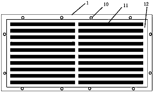
[0027] S1: if image 3 As shown, 20 antenna PCB11 are arranged in a matrix on the large board body 1, and the upper and lower adjacent antenna PCB11 are set as a unit 2. The four sides of the antenna PCB11 are surrounded by the part to be processed 12, and are located near the frame of the large board body 1. Positioning holes 10 are set;

[0028] S2: For the first slot milling, use a CNC machine tool to mill a slot on the part 12 to be processed on the ...


PUM


Abstract

The invention discloses a shape processing method for a PTFE antenna PCB product without internal positioning narrow edges. The shape processing method is suitable for an ultra-narrow antenna PCB madeof a PTFE-based material, can ensure that the antenna PCB is qualified in size, has no oxides and no burr defects after the shape processing, guarantees product quality and eradicates the defects oftoo large or too small size caused by shape processing.

Description

technical field [0001] The invention relates to the field of PCB manufacturing, in particular to a method for processing the shape of a PCB product with a narrow side and no inner positioning PTFE material antenna. Background technique [0002] 5G applications will gradually increase from 3GHz to 6GHz or even higher 30GHz frequency to transmit high-speed signals, which will bring new technical challenges to the manufacture and processing of antenna radio frequency materials. PTFE has excellent dielectric properties, chemical corrosion resistance and high and low temperature resistance, so PTFE is the most ideal material for processing high-frequency antenna PCB products, because the number and complexity of 5G Massive MiMO antennas are far away The active antenna system, which is much higher than the previous 4G, needs to integrate more products in a smaller size space, so it also puts forward higher requirements for the processing of materials. [0003] For ordinary rigid ...

Claims


Application Information

Patent Timeline
Patent Type & Authority Applications(China)
IPC IPC(8): H05K3/00
Inventor 武守坤林鹭华聂兴培陈春樊廷慧唐宏华
Owner HUIZHOU KING BROTHER CIRCUIT TECH
Why Eureka
Try Eureka