
Optical module packaging structure and optical module

A packaging structure and optical module technology, applied in the coupling of optical waveguides, etc., can solve the problems of increasing thermal resistance, narrow product operating temperature range, and difficulty in dissipating module heat, reducing thermal resistance, enhancing thermal conduction efficiency, and solving heat dissipation problems. effect of the problem

Inactive Publication Date: 2019-06-07
HISENSE & JONHON OPTICAL ELECTRICAL TECH CO LTD
View PDF6 Cites 11 Cited by
  • Summary
  • Abstract
  • Description
  • Claims
  • Application Information

AI Technical Summary

Problems solved by technology

At present, although such miniaturized photoelectric conversion module products appearing on the market are miniaturized in terms of external dimensions, they are limited by space squeeze and have no reasonable design of heat dissipation channels, so it is difficult to dissipate heat from the modules.
At present, the common packaging structure is to directly mount the chip on the PCB board, and then install the optical component and the housing. The thermal conductivity of the PCB board is poor, and the chip cannot effectively dissipate heat downward. There is a large air gap or thermal paste, which increases the thermal resistance and reduces the thermal conductivity, so that the chip cannot dissipate heat directly through the housing. Although most of the existing optical modules will eventually mount a heat sink on the housing, it is expected that the module The upper surface realizes high-efficiency heat dissipation, but the heat dissipation effect is not ideal. Therefore, this type of packaging structure does not solve the problem of module heat dissipation, resulting in a narrow operating temperature range of the product.

Method used


Image

  • Optical module packaging structure and optical module
  • Optical module packaging structure and optical module
  • Optical module packaging structure and optical module

Examples


Embodiment Construction

[0032] The specific implementation manners of the present invention will be further described in detail below in conjunction with the accompanying drawings.

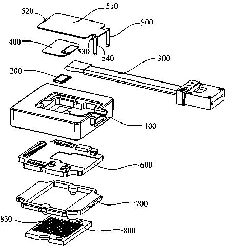
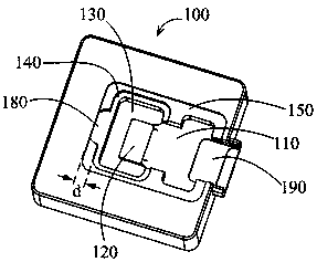
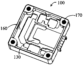
[0033] This embodiment is aimed at chips (such as optical transceiver chips, driver chips, etc.) that easily generate heat during the working process of optical modules (such as optical transmitting modules, optical receiving modules, or optical transceiver modules, etc.). Fast, and when the temperature reaches the limit value, the performance of the chip will deteriorate or stop running directly, affecting the normal operation of the optical module). ), a high-efficiency heat dissipation optical module packaging structure is proposed, such as figure 1 As shown, it includes the metal shell 100, the top cover 500, the bottom plate 700 and other main components, which are used to package the chip 200 in the optical module, the circuit board 600, the optical connector 310 at the front end of the optical component 300, and a...


PUM


Abstract

The invention discloses an optical module packaging structure, which includes a top cover, a bottom plate and a metal shell. An accommodating cavity for accommodating an electrical coupler is formed in the bottom plate, a bottom groove is formed in the bottom of the metal shell for accommodating a circuit board and the bottom plate, and the bottom plate is attached to the surface, away from the top of the metal shell, of the circuit board; and a top groove is formed in the top of the metal shell, the top cover is used for covering the top groove, a part of the groove bottom of the top groove forms a chip carrying part for carrying a chip, and a through groove communicating the bottom groove with the top groove is formed in the position near the chip carrying part. According to the opticalmodule packaging structure, the chip makes a direct contact with the metal shell, a metal heat dissipation channel to the metal shell is formed, heat generated by chip operation diffuses to the outerside of the metal shell through the heat dissipation channel, an air gap between the chip and the metal shell is removed, thermal resistance between the chip and the shell is effectively reduced, andheat dissipation of an optical module is enhanced.

Description

technical field [0001] The invention belongs to the technical field of photoelectric conversion devices, and in particular relates to a packaging structure of an optical module and the optical module. Background technique [0002] With the rapid promotion and in-depth application of optical communication technology, the demand for photoelectric conversion modules is increasing day by day, and the market demand is also developing in the direction of continuous miniaturization, high speed, high density, and high power, but this brings about module heat concentration. And it is difficult to dissipate heat, which affects the product performance and lifespan of the photoelectric conversion module. [0003] The heat generated by the photoelectric conversion module mainly comes from internal chips, such as optical transceiver chips and driver chips. At present, although such miniaturized photoelectric conversion module products appearing on the market are miniaturized in terms of ...

Claims


Application Information

Patent Timeline
IPC IPC(8): G02B6/42
Inventor 仲兆良魏伦王永乐郭琦
Owner HISENSE & JONHON OPTICAL ELECTRICAL TECH CO LTD
Features
  • Generate Ideas
  • Intellectual Property
  • Life Sciences
  • Materials
  • Tech Scout
  • Unparalleled Data Quality
  • Higher Quality Content
  • 60% Fewer Hallucinations
Learn More