Process for coating the surface of a solid substrate with a layer comprising a ceramic compound and the coated substrate obtained

A technology of solid substrates and compounds, applied in the direction of plating, coating, support elements of blades, etc. of superimposed layers, capable of solving different problems

Active Publication Date: 2021-07-16
COMMISSARIAT A LENERGIE ATOMIQUE ET AUX ENERGIES ALTERNATIVES +1
View PDF11 Cites 0 Cited by
  • Summary
  • Abstract
  • Description
  • Claims
  • Application Information

AI Technical Summary

Problems solved by technology

[0028] However, it has been found that in the CMAS-resistant layer obtained by SPS, there are penetration points of CMAS contaminants through the layer, so that the penetration of CMAS contaminants at the core of the coating under the CMAS-resistant layer is very significant, which is different from that with Sediments such as APS technology

Method used


Image

  • Process for coating the surface of a solid substrate with a layer comprising a ceramic compound and the coated substrate obtained
  • Process for coating the surface of a solid substrate with a layer comprising a ceramic compound and the coated substrate obtained
  • Process for coating the surface of a solid substrate with a layer comprising a ceramic compound and the coated substrate obtained

Examples


no. 1 approach

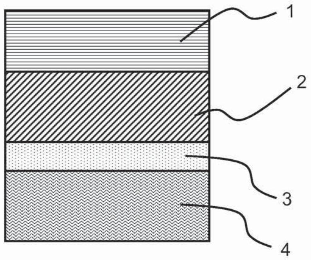
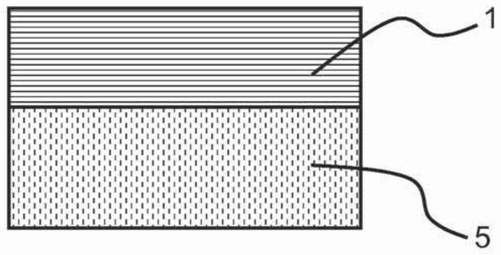
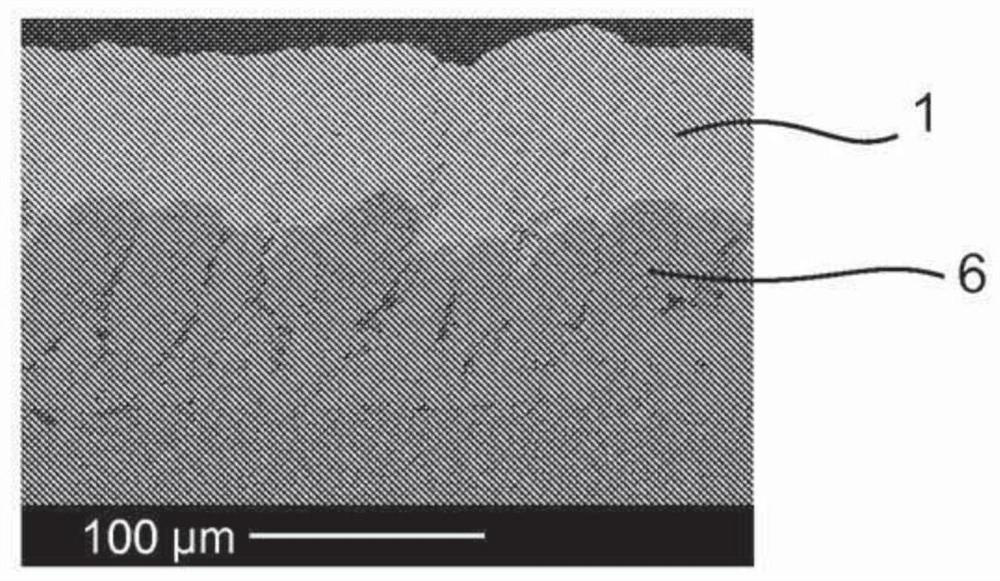
[0155] According to a first embodiment, a layer 1 according to the invention can be applied to a layer 2 obtained by SPS with a porous columnar microstructure ( image 3 Layer 6) in the middle.

[0156] According to a second embodiment, a layer 1 according to the invention can be applied to a layer 2 obtained by SPS with a porous dense columnar microstructure ( Figure 4 Layer 7) in the middle.

[0157] According to a third embodiment, a layer 1 according to the invention can be applied to a layer 2 with a columnar microstructure obtained by EB-PVD ( Figure 5 on layer 8) in

[0158] Advantageously, layer 2 can have a thermal and / or environmental insulation function. This layer can also (but is not limited to) guarantee good properties in terms of service life, thermal insulation or protection against oxidation and moisture corrosion.

[0159] Advantageously, layer 3 acts as an adhesive layer.

[0160] Layer 3 may be selected from metals; metal alloys such as β-NiAl metal a...

Embodiment 1

[0187] In this embodiment, the anti-CMAS layer according to the invention is prepared by the method according to the invention (see image 3 ).

[0188] by Gd 2 Zr 2 o 7 The compositional anti-CMAS layer 1 is prepared on the surface of the porous columnar YSZ layer 6 obtained by the SPS method. By the SPS method using d 90 Less than 10μm (ie d 90 is 7μm) and d 50 A suspension of primary particles greater than or equal to 1 μm (ie 3 μm) was used to prepare the anti-CMAS layer.

[0189] A sample thus prepared consisting of an anti-CMAS layer on a substrate fell into figure 1 and figure 2 within the range of the system shown.

[0190] image 3 A scanning electron microscope (SEM) micrograph using backscattered electrons using a polished portion of the sample prepared in this example is shown.

Embodiment 2

[0192] In this example, the anti-CMAS layer according to the invention was produced by the method according to the invention.

[0193] by Gd 2 Zr 2 o 7 The compositional anti-CMAS layer 1 was prepared on the surface of the columnar dense porous YSZ layer 7 obtained by the SPS method. By the SPS method using d 90 Less than 10μm (ie d 90 is 7μm) and d 50 A suspension of primary particles greater than or equal to 1 μm (ie 3 μm) was used to prepare the anti-CMAS layer.

[0194] A sample thus prepared consisting of an anti-CMAS layer on a substrate fell into figure 1 and figure 2 within the range of the system shown.

[0195] Figure 4 A scanning electron microscope (SEM) micrograph using backscattered electrons using a polished portion of the sample prepared in this example is shown.


PUM

PropertyMeasurementUnit
sizeaaaaaaaaaa
thicknessaaaaaaaaaa
thicknessaaaaaaaaaa

Abstract

The present invention relates to a method for coating at least one surface of a solid substrate with at least one layer comprising at least one ceramic compound by the technique of Suspension Plasma Spraying (SPS), wherein at least one solid particle of at least one ceramic compound injecting the suspension into a plasma jet and subsequently projecting a hot jet containing the solid particle suspension onto the surface of the substrate, whereby a layer containing at least one ceramic compound is formed on the surface of the substrate; the method is characterized in that, at In the suspension, at least 90vol% of the solid particles have a larger size (called d 90 ), such as a diameter of less than 15 μm, preferably less than 10 μm, and at least 50 vol% of the solid particles have a larger size, such as diameter (referred to as d 50 ) is not less than 1 μm. The invention also relates to a substrate coated with at least one layer obtained by the method. The invention also relates to components comprising said coated substrate. The invention also relates to the use of said layer to protect solid substrates from degradation caused by contaminants such as CMAS.

Description

technical field [0001] The invention relates to a method for coating at least one surface of a solid substrate with at least one layer comprising at least one ceramic compound. [0002] Said layer is in particular a layer capable of resisting penetration and degradation at high temperatures by pollutants, in particular in the form of solid particles such as dust, sand or ash. Specifically, these pollutants can be composed of lime (CaO), magnesium oxide (MgO), aluminum oxide (Al 2 o 3 ) and silicon oxide (SiO 2 ) is composed of a mixture of oxides. These pollutants are commonly referred to as CMAS. [0003] The invention further relates to a solid substrate coated with a layer obtainable by the coating method according to the invention. [0004] The invention also relates to components comprising said solid substrate. [0005] More specifically, the layers prepared by the method according to the invention are intended to be integrated in multilayer coatings protecting sol...

Claims


Application Information

Patent Timeline
Patent Type & Authority Patents(China)
IPC IPC(8): C23C4/10C23C4/12C23C28/04C23C28/00F01D5/02F01D5/06F01D5/12C23C4/11C23C4/134
CPCC23C4/10C23C4/12C23C28/042C23C28/048C23C28/3215C23C28/3455C23C4/134F01D5/288F05D2300/15F05D2300/6033F05D2230/312F05D2300/2118F05D2300/2112C23C4/11F01D9/04F05D2230/90
Inventor 本杰明·伯纳德奥雷利·凯特伊曼纽尔·埃尔韦卢克·比安基奥勒里安·朱莉娅安德烈·马利
Owner COMMISSARIAT A LENERGIE ATOMIQUE ET AUX ENERGIES ALTERNATIVES
Why Eureka
Try Eureka