Three-dimensional memory and manufacturing method thereof

A manufacturing method and memory technology, applied in the direction of electric solid-state devices, semiconductor devices, electrical components, etc., can solve the problems of poor performance of three-dimensional memory, and achieve the effects of enhancing stability and improving programming and erasing performance

Active Publication Date: 2019-06-14
YANGTZE MEMORY TECH CO LTD
View PDF8 Cites 6 Cited by
  • Summary
  • Abstract
  • Description
  • Claims
  • Application Information

AI Technical Summary

Problems solved by technology

[0005] The invention provides a three-dimensional memory and its manufacturing method, which are used to solve the problem of poor performance of the three-dimensional memory in the prior art due to the direct contact between the end surface of the bottom of the charge trapping layer and the channel layer

Method used


Image

  • Three-dimensional memory and manufacturing method thereof
  • Three-dimensional memory and manufacturing method thereof
  • Three-dimensional memory and manufacturing method thereof

Examples


no. 1 Embodiment approach

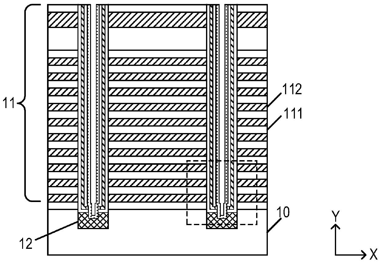
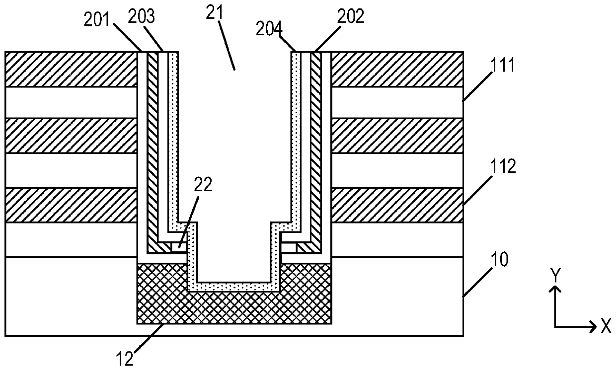
[0056] In three-dimensional memories such as 3D NAND, the storage unit as its key storage structure is composed of a storage string (that is, a NAND string) and its corresponding gate, wherein the storage string includes sequentially stacked gates along the radial direction of the channel hole. Barrier layer, charge trapping layer, tunneling layer and channel layer. After completing the deposition of the blocking layer, the charge trapping layer and the tunneling layer in the channel hole, the blocking layer, the charge trapping layer and the tunneling layer are etched to open the The bottom of the channel hole is exposed to expose the epitaxial semiconductor layer; and then the channel layer is deposited to form a channel channel.

[0057]As the market's requirements for storage density continue to increase, the number of stacked layers in the stacked structure in the three-dimensional memory continues to increase, which leads to a corresponding reduction in the size of the c...

no. 2 Embodiment approach

[0094] This specific embodiment provides a three-dimensional memory and its manufacturing method, with Figure 5 It is a structural schematic diagram of the three-dimensional memory in the second specific embodiment of the present invention. For the same parts as the first specific embodiment, this specific embodiment will not repeat it, and the differences from the first specific embodiment will be mainly described below.

[0095] Such as Figure 5 As shown, the three-dimensional memory provided in this specific embodiment includes:

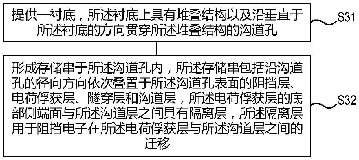
[0096] a substrate 50, on which there is a stack structure and a channel hole penetrating through the stack structure along a direction perpendicular to the substrate 50;

[0097] The storage string, located in the channel hole, includes a blocking layer 521, a charge trapping layer 522, a tunneling layer 523 and a channel layer 524 stacked on the surface of the channel hole in sequence along the radial direction of the channel hole;

[0098]...


PUM


Abstract

The invention relates to the technical field of semiconductor manufacturing, in particular to a three-dimensional memory and a manufacturing method thereof. The three-dimensional memory comprises a substrate, a storage string and an isolation layer, wherein the substrate is provided with a stacking structure and a channel hole which penetrates through the stacking structure in a direction perpendicular to the substrate; the storage string is located in the channel hole and comprises a blocking layer, a charge trapping layer, a tunneling layer and a channel layer which are sequentially stackedon the surface of the channel hole in the radial direction of the channel hole; and the isolation layer is positioned between the side end surface of the bottom of the charge trapping layer and the channel layer, and is used for blocking the migration of electrons between the charge trapping layer and the channel layer. According to the three-dimensional memory, direct contact between the channellayer and the charge trapping layer is avoided, the migration of charges between the channel layer and the charge trapping layer is blocked, and the writing and erasing performance of the three-dimensional memory can be effectively improved.

Description

technical field [0001] The invention relates to the technical field of semiconductor manufacturing, in particular to a three-dimensional memory and a manufacturing method thereof. Background technique [0002] As technology develops, the semiconductor industry is constantly seeking new ways to produce a greater number of memory cells per memory die in a memory device. In non-volatile memory, such as NAND memory, one way to increase the memory density is by using vertical memory arrays, that is, 3D NAND (three-dimensional NAND) memory; 32 layers developed to 64 layers, or even higher layers. [0003] In a 3D NAND memory, there is a stack structure formed by alternately stacking interlayer insulating layers and gates, and the stack structure includes a core area and a stepped area surrounding the core area. The core area is used for storing information; the step area is located at the end of the stack structure and is used for transmitting control information to the core are...

Claims


Application Information

Patent Timeline
Patent Type & Authority Applications(China)
IPC IPC(8): H01L27/11582
Inventor 王启光张安
Owner YANGTZE MEMORY TECH CO LTD
Why Eureka
Try Eureka