Display substrate, manufacturing method thereof and display device

A technology for displaying substrates and substrates, which is applied in the fields of final product manufacturing, sustainable manufacturing/processing, semiconductor/solid-state device manufacturing, etc., and can solve problems such as high manufacturing costs, difficult design, and difficult process realization

Active Publication Date: 2019-06-25
BOE TECH GRP CO LTD
View PDF5 Cites 67 Cited by
  • Summary
  • Abstract
  • Description
  • Claims
  • Application Information

AI Technical Summary

Problems solved by technology

[0006] The technical problem to be solved by the embodiments of the present invention is to provide a display substrate and its preparation method, and a displ

Method used


Image

  • Display substrate, manufacturing method thereof and display device
  • Display substrate, manufacturing method thereof and display device
  • Display substrate, manufacturing method thereof and display device

Examples


Embodiment Construction

[0053] The specific implementation manners of the present invention will be further described in detail below in conjunction with the accompanying drawings and examples. The following examples are used to illustrate the present invention, but are not intended to limit the scope of the present invention. It should be noted that, in the case of no conflict, the embodiments in the present application and the features in the embodiments can be combined arbitrarily with each other.

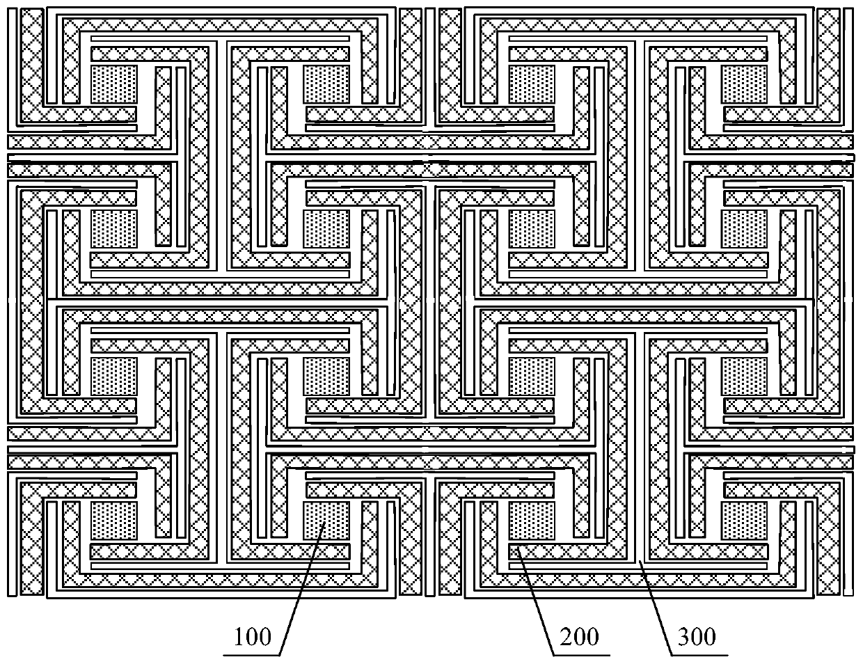
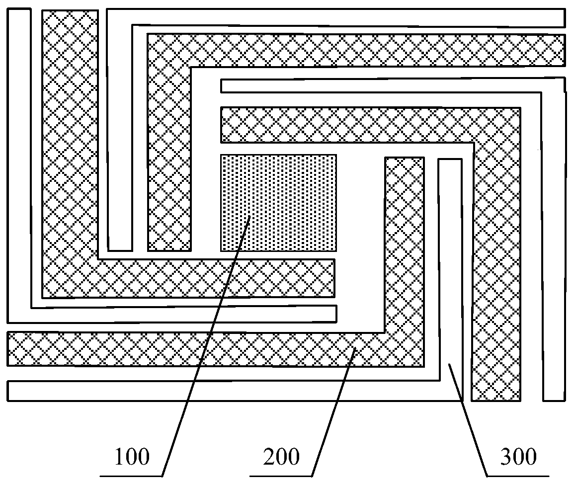
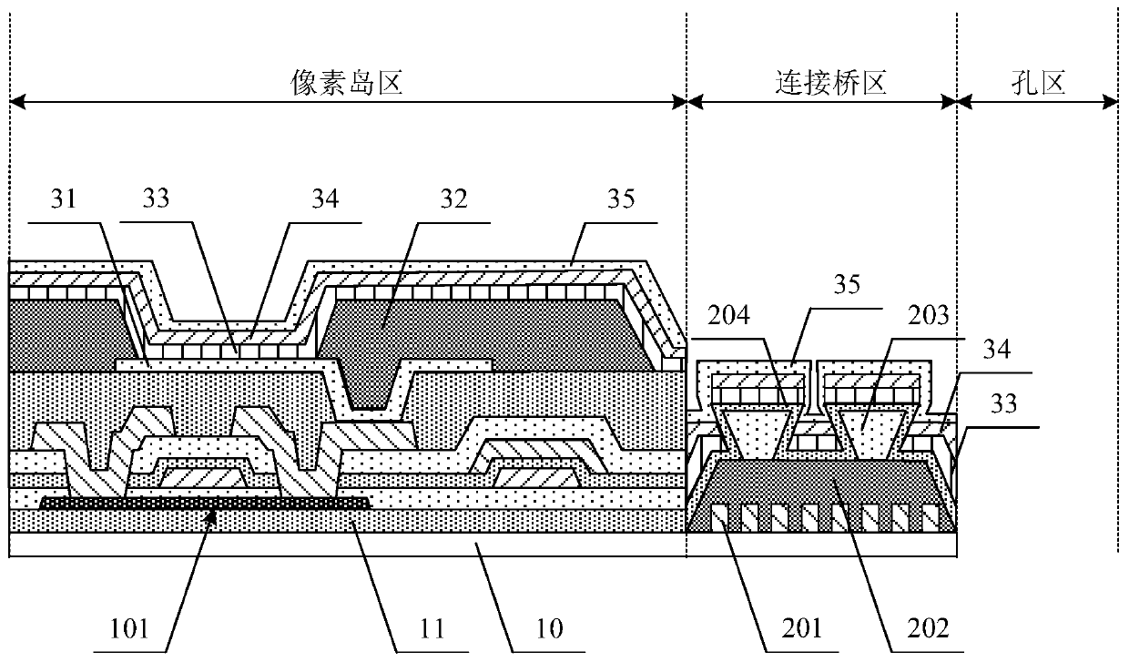
[0054] In order to solve the problems of difficult design, high manufacturing cost, and difficult process realization existing in the existing packaging solutions, the embodiments of the present invention provide a display substrate and its preparation method, and a display device, which do not require the use of organic light-emitting layers and cathode patterning. The process has the advantages of low design difficulty, low manufacturing cost, easy process realization, and effective guarantee of the ef...


PUM

PropertyMeasurementUnit
Heightaaaaaaaaaa
Widthaaaaaaaaaa
Widthaaaaaaaaaa

Abstract

The invention provides a display substrate, a manufacturing method thereof and a display device. The display substrate includes a substrate, a plurality of pixel island regions arranged in an array onthe substrate and spaced apart from each other, a plurality of hole regions, and connection bridge regions located between the pixel island regions and the hole regions, wherein each connection bridge region is provided with a partition structure layer for disconnecting an organic light emitting layer and a cathode of the connection bridge region. As the partition structure lay is arranged in each connection bridge region and the partition structure layer disconnects the organic light emitting layer and the cathode of the connection bridge region, a water vapor intrusion path intruding to theorganic light emitting layer and the cathode in the pixel island region from the hole region can be completely blocked, the validity and the reliability of packaging are effectively ensued, the design difficulty is low, the manufacturing cost is low, process realization is easy, and the problems of high design difficulty, high manufacturing cost and difficult process realization existing in the current packaging scheme can be effectively solved.

Description

technical field [0001] The invention relates to the field of display technology, in particular to a display substrate, a preparation method thereof, and a display device. Background technique [0002] Organic Light Emitting Diode (OLED) is an active light-emitting display device, which has the advantages of self-illumination, wide viewing angle, high contrast, low power consumption, and extremely high response speed. With the continuous development of display technology, OLED technology is more and more applied to flexible display devices, and the flexible display device is gradually developing from a two-dimensional direction-variable mode to a three-dimensional direction-variable mode. [0003] Currently, flexible OLED display devices usually adopt an island-bridge structure. The island bridge structure is that the light-emitting units are arranged in the pixel island area, and the connecting lines between the pixel islands are arranged in the connecting bridge area. When...

Claims


Application Information

Patent Timeline
IPC IPC(8): H01L51/52H01L27/32H01L21/77
CPCH01L21/77Y02P70/50H10K59/131H10K50/844H10K71/00H10K77/111H10K50/11H10K50/82H10K59/122H10K59/1201H10K71/80H10K2102/311
Inventor 谢春燕张嵩张子予秦成杰王品凡谷朋浩
Owner BOE TECH GRP CO LTD
Why Eureka
Try Eureka