A programmable logic unit structure and a chip

A logic unit and programming logic technology, applied in the direction of instruments, electrical digital data processing, digital data processing components, etc., can solve the problems of less combination logic and addition logic, low resource area utilization efficiency, and large number of input ports, etc., to achieve The effect of improving logic efficiency, optimizing area utilization, and improving mapping efficiency

Active Publication Date: 2019-06-28
SHANGHAI ANLOGIC INFOTECH CO LTD
View PDF5 Cites 4 Cited by
  • Summary
  • Abstract
  • Description
  • Claims
  • Application Information

AI Technical Summary

Problems solved by technology

This single LE structure wastes too many input ports when implementing addition and subtraction logic, resulting in a lot of unused interconnection resources, less combinational logic and addition logic that can be realized per unit chip area, and low resource area utilization efficiency

Method used


Image

  • A programmable logic unit structure and a chip
  • A programmable logic unit structure and a chip
  • A programmable logic unit structure and a chip

Examples


Embodiment Construction

[0050] In the following description, many technical details are proposed in order to enable readers to better understand the application. However, those skilled in the art can understand that even without these technical details and various changes and modifications based on the following embodiments, the technical solutions claimed in this application can also be realized.

[0051] Explanation of some concepts:

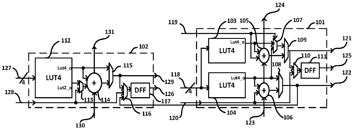
[0052] Programmable logic cell: In a programmable logic device, a programmable logic cell is usually used to implement random logic functions and sequential logic in user designs. For Field Programmable Logic Array (FPGA), most programmable logic units are composed of a certain number of look-up tables and sequential units (edge-triggered registers or level-type latches). The programmable logic cells are connected together through pre-customized metal wiring and controllable switches (programmable interconnection).

[0053] Logic unit: Logic Element, referred to as...


PUM


Abstract

The invention relates to the field of integrated circuit design, and discloses a programmable logic unit structure and a chip. The programmable logic unit structure comprises a first logic unit LE5 and a second logic unit LE4. The LE4 and the LE5 are mixed to form a programmable logic pair structure, a plurality of programmable logic pair structures are combined to form a programmable logic blockstructure, and carry chains of the LE4 in adjacent programmable logic pairs are connected to form an N-bit traveling wave addition; And carry chains of LE5 in adjacent programmable logic pairs are connected to form 2N-bit traveling wave addition. In practical application, common logic can be achieved through LE4 mapping, multi-output logic and arithmetic operation under the same input condition are achieved through LE5 mapping, and the balance of the resource area utilization rate and flexibility is achieved.

Description

technical field [0001] This application relates to the field of integrated circuit design, in particular to the technology of programmable logic unit structure design. Background technique [0002] Multiple LEs of the same structure are used in most FPGA architectures combined in one programmable logic block. Most resources such as traditional commercial FPGAs. LE4 is generated by a logic function based on a simple four-input look-up table structure and a full add. device and a DFF form. A programmable logic block contains N LE4s, such as N=8. This single LE structure wastes too many input ports when implementing addition and subtraction logic, resulting in a lot of unused interconnection resources, less combinatorial logic and addition logic that can be realized per unit chip area, and low resource area utilization efficiency. Contents of the invention [0003] The purpose of this application is to provide a programmable logic unit structure and chip, which can simplify...

Claims


Application Information

Patent Timeline
Patent Type & Authority Applications(China)
IPC IPC(8): G06F7/575G06F7/501G06F7/505
Inventor 王元
Owner SHANGHAI ANLOGIC INFOTECH CO LTD
Why Eureka
Try Eureka