Method for transferring MICRO LED chips out of and into panel from wafer
A chip transfer and chip technology, applied in the manufacturing of instruments, electrical components, semiconductor/solid-state devices, etc., can solve problems such as difficulty in mass production, and achieve the effect of precise matching of binding points, expansion of distance, and no waste of area.
- Summary
- Abstract
- Description
- Claims
- Application Information
AI Technical Summary
Problems solved by technology
Method used
Image

Examples
Embodiment 1
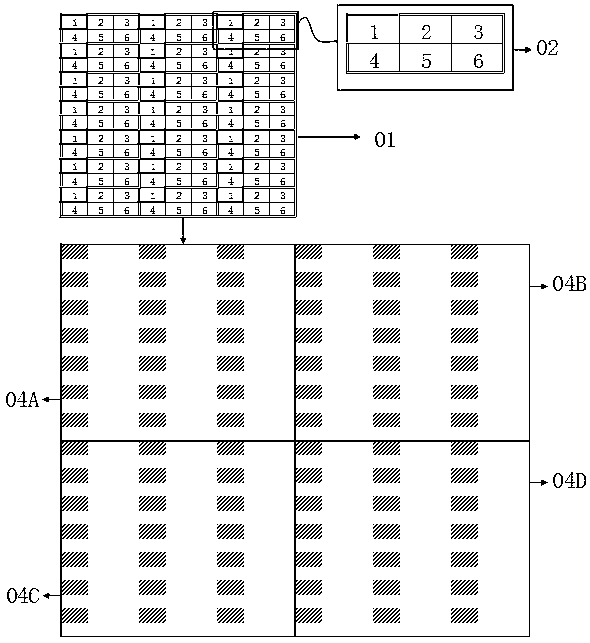
[0047] Such as figure 2 As shown, after the entire process of the MICRO LED chip is completed on the wafer, the single MICRO LED chip is not split, but the first unit is divided by multiple quantitative MICRO LED chips in the same area (not necessarily the actual division, you can Virtual), the wafer is divided into multiple chip sets with the same area, the same shape, and an equal number of MICRO LED chips, that is, multiple first units, and are split in units of the first unit, and multiple independent chips are separated from the wafer. the first unit of . In the present invention, splitting is carried out in units of the first unit so that the first unit on the wafer is separated from the wafer, which is defined as the first transfer of the MICRO LED chip, that is, it is transferred from the wafer, but the MICRO LED chip is still on the first unit. After the first unit of the chip set of the MICRO LED chip is separated from the wafer, the second unit is defined on the ...
Embodiment 2
[0049] As in Example 1, the first unit is prepared, the first transfer of the MICRO LED chip is completed, the second unit is defined to start the second transfer of the MICRO LED chip, and the second unit is used as a unit to perform the second first transfer of the MICRO LED chip , one MICRO LED chip on each second unit in the first unit is transferred to the temporary substrate, such as Figure 9 As shown, the MICRO LED chip at position A of each second unit is fixed on the temporary substrate, such as Figure 10 It is shown that the MICRO LED chips in position A of each second unit are peeled off from the first unit by laser. Fix the P electrode of the MICRO LED chip at position A on the temporary substrate; Figure 11 As shown, the MICRO LED chip at position B of each second unit is fixed on the temporary substrate, such as Figure 12 As shown, the MICRO LED chips in position B of each second unit are peeled off from the first unit by laser. The P electrode of the MICR...
Embodiment 3
[0051] The first unit is prepared as in Embodiments 1 and 2, and the first transfer of the MICRO LED chip is completed. The first transfer of the second MICRO LED chip is completed as in Embodiment 2. The required MICRO LED chip has been transferred to the temporary substrate. The MICRO LED chip on the temporary substrate is divided into units according to the chip set, which is defined as the chip set unit X. One MICROLED chip on each unit is transferred to another temporary substrate A. During the same transfer process of the MICRO LED chip, each unit is transferred The rolled-out MICRO LED chips are located at the same position in each unit. Such as Figure 16 As shown, the MICRO LED chip at position A of each chip set unit X is fixed on the temporary substrate X, and the process of the MICRO LED chip at other positions of each chip set unit X is the same as above. The temporary substrate X is matched with the panel at a ratio of 1:1, and all the MICRO LED chips on the tem...
PUM
 Abstract
Description
Claims
Application Information
 - R&D
- Intellectual Property
- Life Sciences
- Materials
- Tech Scout
- Unparalleled Data Quality
- Higher Quality Content
- 60% Fewer Hallucinations
Browse by: Latest US Patents, China's latest patents, Technical Efficacy Thesaurus, Application Domain, Technology Topic, Popular Technical Reports.
© 2025 PatSnap. All rights reserved.Legal|Privacy policy|Modern Slavery Act Transparency Statement|Sitemap|About US| Contact US: help@patsnap.com