

OLED display panel and manufacturing method thereof, and OLED display device
A display panel and display layer technology, applied in the direction of electrical components, electrical solid devices, circuits, etc., can solve problems such as adverse effects of white balance, and achieve the effect of alleviating the problem of color cast
- Summary
- Abstract
- Description
- Claims
- Application Information
AI Technical Summary
Problems solved by technology
Method used
Image


Examples
Embodiment 1
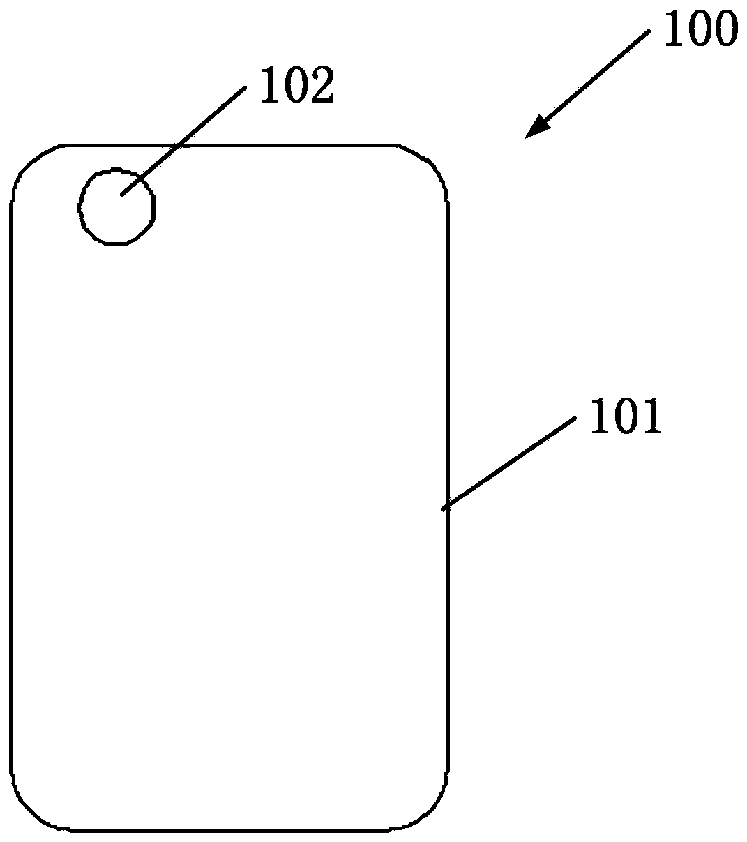
[0038] Such as figure 1 As shown, an OLED display panel 100 is defined with a first display area and a second display area. These include: .
[0039] Such as figure 2 As shown, it includes: a substrate 1 , a driving display layer 2 , a cover 3 and an optical balance layer 4 . Wherein the driving display layer 2 is disposed on the substrate 1; the cover plate 3 is disposed on the driving display layer 2; the optical balance layer 4 is disposed on the substrate 1 of the second display area 102 away from all One side of the display layer 2 is driven.
[0040] Such as image 3 As shown, since the substrate 1 includes a polyimide layer, wherein the polyimide layer has a transmittance greater than 40% for visible light with a wavelength greater than 450 nm, further, the polyimide layer has a wavelength greater than 450 nm. The transmittance of visible light at 450nm is greater than 50%. Therefore, when the light that drives the display layer 2 passes through the substrate 1 ,...
Embodiment 2
[0045] Such as Figure 5 As shown, this embodiment provides a method for preparing the OLED display panel 100 involved in the present invention, which includes:
[0046] Step S1, defining a first display area 101 and a second display area 102 on the OLED display panel 100 to be prepared, providing a substrate 1, and preparing a driving display layer 2 on the substrate 1;
[0047] Step S2, preparing a cover plate 3 on the driving display layer 2;
[0048] Step S3 , disposing an optical balance layer 4 on the side of the substrate 1 of the second display area 102 away from the driving display layer 2 .
[0049] Further, in the step S3, the optical balance layer 4 is formed by coating on the side of the substrate 1 of the second display area 102 away from the driving display layer 2 by means of chemical deposition or physical deposition.
Embodiment 3
[0051] Such as Figure 6 As shown, the present invention also provides an OLED display device, which includes: the OLED display panel 100 designed in the present invention and the camera 5, the camera 5 is correspondingly arranged on the side of the optical balance layer 4 away from the substrate 1 . In this way, the optical balance layer 4 can perform a transmittance balance compensation function, thereby reducing the color cast problem of the overall transmitted light and improving the white balance of the image captured by the camera 5 .
PUM
 Abstract
Description
Claims
Application Information