
Display device

A display device and display area technology, which is applied in nonlinear optics, instruments, optics, etc., can solve problems such as the reduction of screen ratio, the inability to export static charges in the display device, and affect the display effect of the display device, so as to reduce antistatic Low cost, full-screen design, simple and convenient settings

Inactive Publication Date: 2019-07-19
XIAMEN TIANMA MICRO ELECTRONICS
View PDF8 Cites 4 Cited by
  • Summary
  • Abstract
  • Description
  • Claims
  • Application Information

AI Technical Summary

Problems solved by technology

[0004] However, the existence of the hole-digging area makes it easy for external static charges to enter the display panel from the hole-digging area, and the hole-digging area is relatively limited. If an electrostatic protection circuit is added in the hole-digging area, it will inevitably lead to a decrease in screen-to-body ratio.
If the electrostatic protection circuit is not installed, the static charge in the display device will not be able to be exported, which will affect the display effect of the display device

Method used


Image

  • Display device
  • Display device
  • Display device

Examples


Embodiment Construction

[0022] The present invention will be further described in detail below in conjunction with the accompanying drawings and embodiments. It should be understood that the specific embodiments described here are only used to explain the present invention, but not to limit the present invention. In addition, it should be noted that, for the convenience of description, only some structures related to the present invention are shown in the drawings but not all structures.

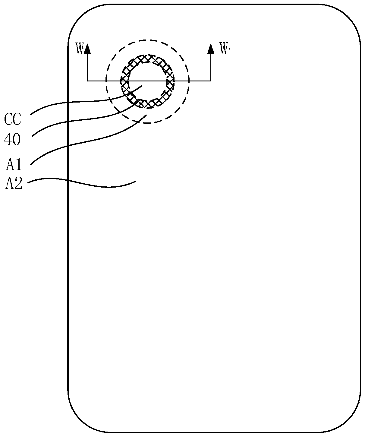
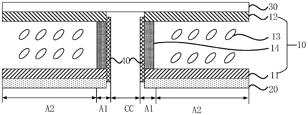
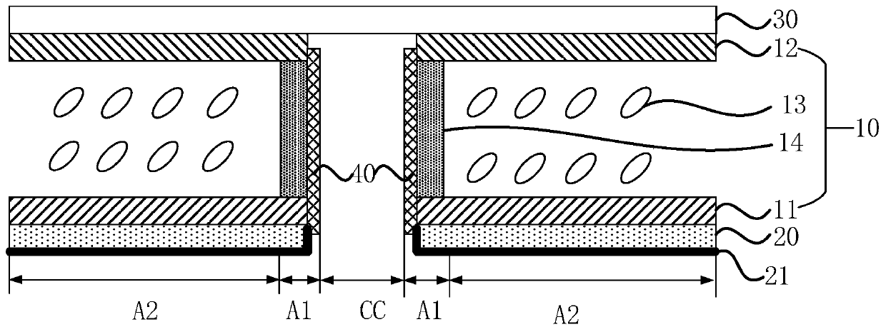
[0023] figure 1 is a schematic plan view of a display device provided by an embodiment of the present invention, figure 2 yes figure 1 Schematic diagram of the cross-sectional structure along the W-W' direction. Please refer to figure 1 and figure 2 As shown, the display device provided by the embodiment of the present invention includes: a hollow part CC, a non-display area A1 and a display area A2; wherein, the non-display area A1 is arranged around the hollow part CC, and the display area A2 is arranged a...


PUM

PropertyMeasurementUnit
electrical resistanceaaaaaaaaaa

Abstract

The invention discloses a display device comprising a hollow part, a non-display area and a display area, wherein the non-display area is arranged around the hollow part, and the display area is arranged around the non-display area; the display device also comprises a display panel, a backlight module and a first conductive structure; the display panel comprises an array substrate and an oppositesubstrate; the backlight module is arranged on one side, with the back to the opposite substrate, of the array substrate; the hollow part penetrates through the display panel and the backlight modulealong a direction perpendicular to the array substrate; the first conductive structure is positioned in the non-display area, and at least covers the array substrate and the surface, close to one sideof the hollow part, of the opposite substrate; one end, far away from the backlight module, of the first conductive structure is electrically connected with the display panel; and one end, facing thebacklight module, of the first conductive structure is electrically connected with the backlight module. By using the display device provided by the embodiment of the invention, the accumulation of electrostatic charges in the display area around the hollow part can be reduced, and the display effect of the display device can be improved.

Description

technical field [0001] Embodiments of the present invention relate to the field of display technologies, and in particular, to a display device. Background technique [0002] Since the full-screen display device has a good visual experience, more and more users pay attention to it. However, how to improve the screen-to-body ratio of the full screen has also become a hot spot in the current development direction. [0003] Currently, for a full-screen display device with a high screen-to-body ratio, due to the need to install light-sensitive devices such as cameras, it is usually designed to dig a hole in the display area of ​​a full-screen display device with a high screen-to-body ratio, and install a camera in the hole-digging area. and other photosensitive devices. [0004] However, the existence of the hole-digging area makes it easy for external electrostatic charges to enter the display panel from the hole-digging area, and the hole-digging area is relatively limited. ...

Claims


Application Information

Patent Timeline
Patent Type & Authority Applications(China)
IPC IPC(8): G02F1/1345
CPCG02F1/1345
Inventor 陈彬彬
Owner XIAMEN TIANMA MICRO ELECTRONICS
Learn More