Semiconductor device

A semiconductor and substrate technology, applied in the field of semiconductor devices, can solve problems such as hindering the movement of carriers

Active Publication Date: 2019-07-19
DENSO CORP
View PDF5 Cites 0 Cited by
  • Summary
  • Abstract
  • Description
  • Claims
  • Application Information

AI Technical Summary

Problems solved by technology

However, in the technique of Patent Document 1, since the impurity concentration in the low-concentration region is lower than that in the collector region and thus the resistance of the low-concentration region is higher than that of the collector region, it is possible that when the IGBT is turned on, hinder the movement of carriers passing through the low concentration region
Therefore, a hysteresis phenomenon may occur in which the current flowing through the IGBT increases after the voltage between the emitter region and the collector region temporarily rises when the IGBT is turned on

Method used


Image

  • Semiconductor device
  • Semiconductor device
  • Semiconductor device

Examples


Deformed example 1

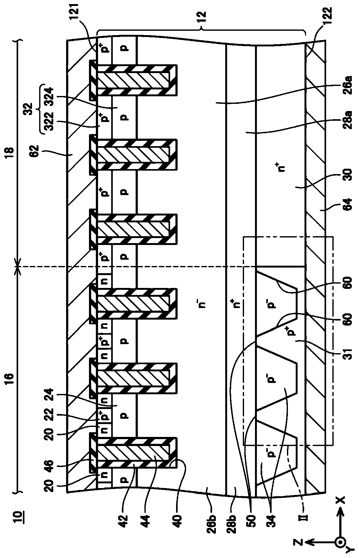
[0045] A modification example will be described. Such as image 3 As shown, in the semiconductor device 10 according to Modification 1, each lateral contact portion 60 (an example of the second contact portion) of each low-concentration region 34 extends in parallel with the direction (Z direction) perpendicular to the semiconductor substrate 12 . in image 3 In the cross section shown, each low concentration region 34 is formed in a rectangular shape.

Deformed example 2

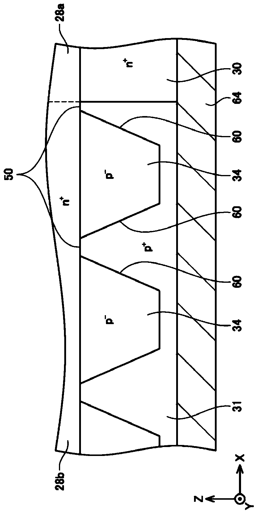
[0047] Such as Figure 4 As shown, in the semiconductor device 10 according to Modification 2, each lateral contact portion 60 of each low-concentration region 34 is curved. Each lateral contact portion 60 of each low-concentration region 34 is curved so as to be convex on the collector region 31 side.

Deformed example 3

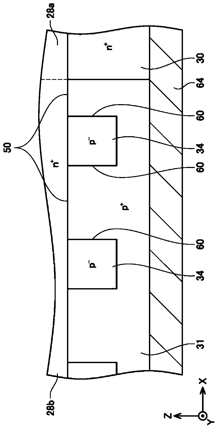
[0049] Such as Figure 5 As shown, in the semiconductor device 10 according to Modification 3, each lateral contact portion 60 of each low-concentration region 34 is curved so as to be convex on the side of each low-concentration region 34.


PUM


Abstract

The present invention provides a technique capable of suppressing a hysteresis phenomenon when an IGBT is turned on while suppressing noises when the IGBT is turned off. A semiconductor substrate mayinclude a diode region and an IGBT region provided adjacent to the diode region. The IGBT region may include a plurality of first conductive-type low concentration regions provided between a buffer region and a collector region, arranged with intervals therebetween in a direction parallel to the semiconductor substrate, and having a lower impurity concentration than the collector region. The collector region may include a contact portion that is in contact with the buffer region between the low concentration regions adjacent to each other.

Description

Technical field [0001] The technology disclosed in this specification relates to a semiconductor device. Background technique [0002] Patent Document 1 discloses an IGBT (Insulating Gate Bi-polar Transistor). The IGBT of Patent Document 1 includes a semiconductor substrate, a surface electrode arranged on the surface of the semiconductor substrate, and a back electrode arranged on the back surface of the semiconductor substrate. In addition, the IGBT of Patent Document 1 further includes an n-type emitter region provided in the range exposed by the surface of the semiconductor substrate, a p-type collector region provided in the range exposed by the back surface of the semiconductor substrate, and the emitter The n-type drift region between the collector region and the collector region, the p-type body region disposed between the emitter region and the drift region, and the depth extending from the surface of the semiconductor substrate through the emitter region and the body r...

Claims


Application Information

Patent Timeline
Patent Type & Authority Applications(China)
IPC IPC(8): H01L29/739H01L29/08H01L29/06
CPCH01L29/7397H01L29/0821H01L29/0634H01L29/407H01L29/8613H01L29/0834H01L27/0716H01L29/0804H01L29/1095H01L29/41708H01L29/4236H01L29/861
Inventor 永井昂哉
Owner DENSO CORP
Why Eureka
Try Eureka