
Substrate defect inspection apparatus, substrate defect inspection method and storage medium

A defect inspection and substrate technology, applied in measuring devices, image data processing, instruments, etc., can solve problems such as insufficient learning

Pending Publication Date: 2019-07-23
TOKYO ELECTRON LTD
View PDF1 Cites 0 Cited by
  • Summary
  • Abstract
  • Description
  • Claims
  • Application Information

AI Technical Summary

Problems solved by technology

Defect classification based on deep learning is learned by using teaching data. However, in the case of insufficient learning, etc., misclassification cannot be avoided.

Method used


Image

  • Substrate defect inspection apparatus, substrate defect inspection method and storage medium
  • Substrate defect inspection apparatus, substrate defect inspection method and storage medium
  • Substrate defect inspection apparatus, substrate defect inspection method and storage medium

Examples


Embodiment Construction

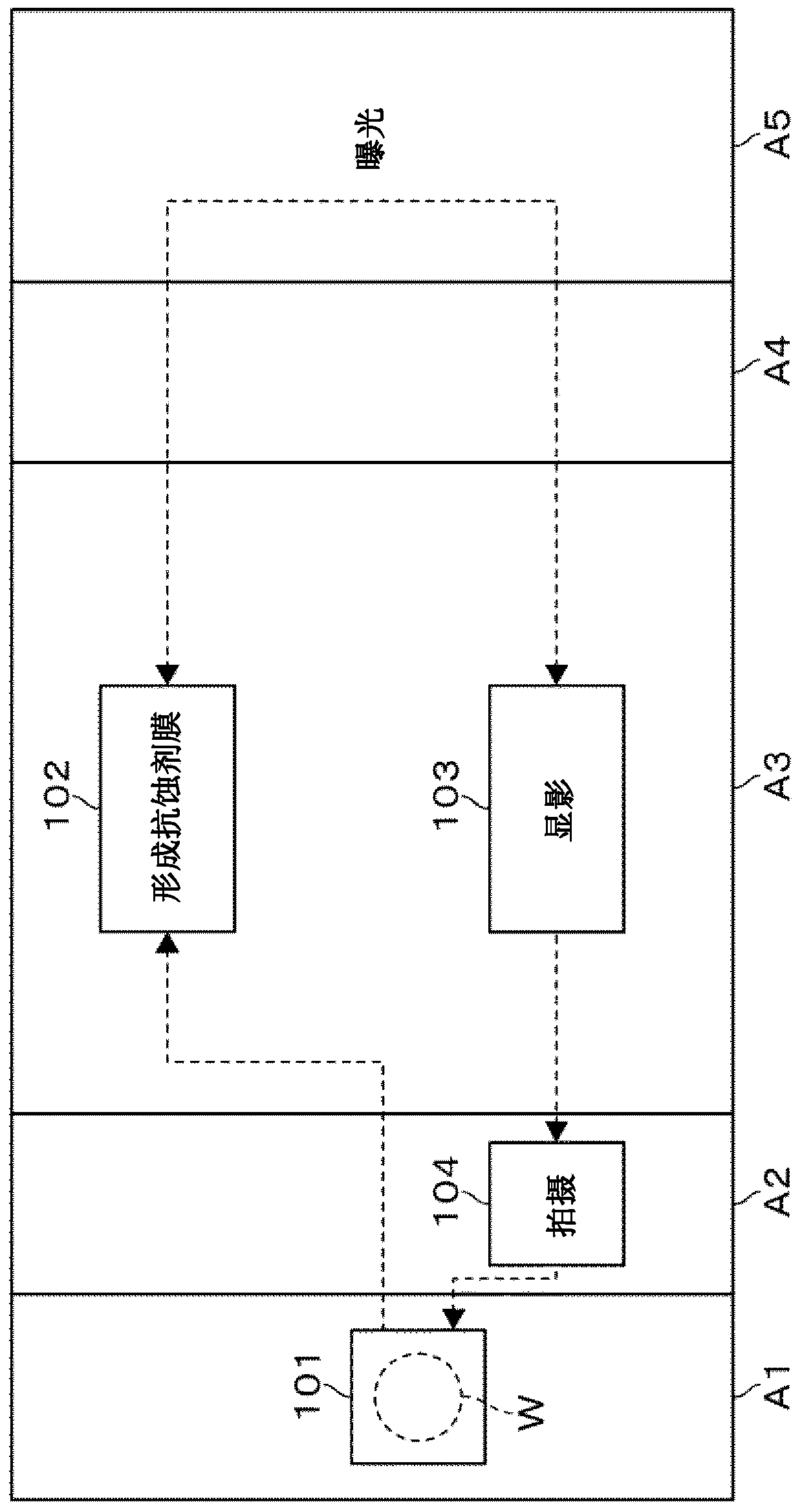
[0057] The substrate defect inspection apparatus of the present invention performs defect inspection based on, for example, an image of a wafer captured by a camera module that can be applied to a coating and developing device that performs resist coating and post-exposure development, and Set in the coating and developing device.

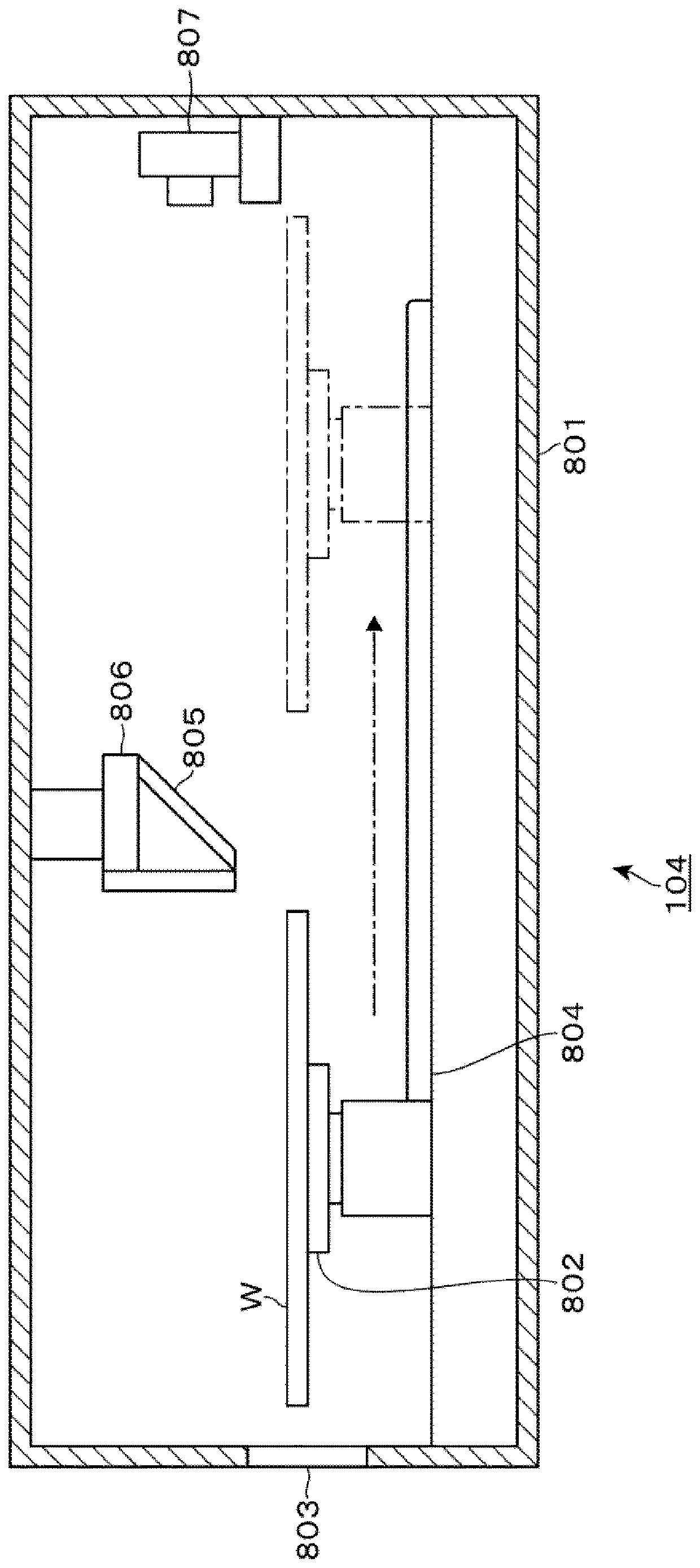
[0058] First, refer to the figure 1, an example of a coating and developing device will be described. The coating and developing device is configured such that the carrier block A1 , the intermediate block A2 , the process block A3 , and the interface block A4 are sequentially connected linearly in the horizontal direction. The interface block A4 is connected with the exposer A5. The carrier 101 containing the wafer W which is a substrate is transported by a carrier transport mechanism not shown and placed on the carrier block A1. The processing block A3 is provided with: a coating module 102 for supplying a resist to the surface of the wafer W ...


PUM


Abstract

The present invention provides a technique capable of appropriately classifying defects of a substrate on the basis of an image of an object to be inspected obtained by imaging the substrate. A solution is to obtain binarized data including a defect region by performing deep learning and a two-class classification unit (3) on a captured image obtained by capturing an image of a substrate. A rectangular color image including a defect region is generated from the binarized data, and the type of the defect is inferred using deep learning based on the image. Furthermore, attributes such as the shape of the defect region and the position on the wafer (W) are determined on the basis of the binarized data, and the type of the defect is estimated using a rule base on the basis of the information.And comprehensively judging the type of the defect based on an inference result of deep learning and an inference result of the rule base.

Description

technical field [0001] The present invention relates to a technique for determining what kind of defect has occurred on a substrate using image data obtained by photographing a substrate. Background technique [0002] In the photolithography step in the manufacturing process of a semiconductor device, a resist film is formed by applying a resist to the surface of a semiconductor wafer (hereinafter referred to as wafer) as a substrate, exposing the resist film, developing , to form a resist pattern. The wafer W after a series of steps is inspected by an inspection device to see whether a good resist pattern is formed on the wafer surface, whether there is a scratch or foreign matter is attached, and the like. Such a defect is called a defect, and the defect has various forms depending on the cause thereof. Therefore, from the viewpoint of semiconductor device manufacturing management, the inspection apparatus is required not only to inspect whether or not a defect occurs on...

Claims


Application Information

Patent Timeline
Patent Type & Authority Applications(China)
IPC IPC(8): H01L21/66H01L21/67
CPCH01L22/12H01L21/67271G06T7/0004G06T7/66G06T2207/30148G06T2207/20132G06T2207/10024G06T2207/20076G06T2207/20084G01N21/9501G01N21/8851G06T7/001H01L21/67288H01L22/30G01B2210/56G06T2207/20081G06T7/0006
Inventor 岩永修儿
Owner TOKYO ELECTRON LTD
Learn More