
pixel circuit

A pixel circuit and writing circuit technology, which is applied in the field of pixel circuits, can solve problems such as current unevenness, achieve the effects of preventing flickering and solving current unevenness

Active Publication Date: 2020-12-01
AU OPTRONICS CORP
View PDF7 Cites 0 Cited by
  • Summary
  • Abstract
  • Description
  • Claims
  • Application Information

AI Technical Summary

Problems solved by technology

[0004] The present invention provides a pixel circuit, which mainly uses an external compensation circuit and a buffer circuit to transmit the compensation voltage to the inside of the pixel circuit for compensation, so as to solve the current inhomogeneity caused by the variation of the critical voltage and prevent the display panel from displaying a black screen. Efficacy of the flickering phenomenon

Method used


Image

  • pixel circuit
  • pixel circuit
  • pixel circuit

Examples


Embodiment Construction

[0042] The embodiments of the present invention will be described below with reference to the relevant drawings. In the drawings, the same reference numbers refer to the same or similar elements or method flows.

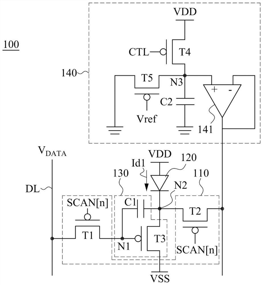
[0043] see figure 1 . figure 1 It is a circuit diagram of a pixel circuit 100 according to an embodiment of the present disclosure. like figure 1 As shown, the pixel circuit 100 includes a data writing circuit 110 , a light emitting diode 120 , a driving circuit 130 and a compensation circuit 140 . The pixel circuit 100 can control the magnitude of the driving current Id1 flowing through the light-emitting diode 120 , so that the light-emitting diode 120 can generate different gray-scale brightness.

[0044] As mentioned above, the writing circuit 110 is electrically coupled to the data line DL, the nodes N1 and N2 for receiving the scan signal SCAN[n] and the data voltage V input from the data line DL DATA . The first end of the light emitting diode 120 is ele...


PUM


Abstract

The invention discloses a pixel circuit which comprises a first data writing circuit, a light emitting diode, a driving circuit and a compensation circuit. The writing circuit is electrically coupledto the data line, the first node and the second node for receiving the scan signal and the data voltage. The light emitting diode is electrically coupled to the second node and used for receiving thefirst voltage. The driving circuit is electrically coupled to the first node, the second node and the second voltage. The compensation circuit is electrically coupled to the write circuit and the second voltage, and is used for receiving the control signal, the first voltage and the reference voltage and outputting the compensation voltage to the write circuit.

Description

technical field [0001] The present disclosure relates to a pixel circuit, and more particularly, to a pixel circuit capable of compensating for variations in threshold voltages of driving transistors. Background technique [0002] Low temperature poly-silicon thin-film transistors (LTPS TFTs) have the characteristics of high carrier mobility and small size, and are suitable for display panels with high resolution, narrow borders and low power consumption. At present, excimer laser annealing (ELA) technology is widely used in the industry to form polysilicon thin films of low temperature polysilicon thin film transistors. However, since the scanning power of each shot of the excimer laser is not stable, the polysilicon film in different regions will have differences in grain size and number. Therefore, in different regions of the display panel, the characteristics of the low temperature polysilicon thin film transistors are different. [0003] For example, low temperature p...

Claims


Application Information

Patent Timeline
Patent Type & Authority Patents(China)
IPC IPC(8): G09G3/32
CPCG09G3/32G09G2320/0233
Inventor 林志隆陈柏勳陈力荣马宏宇郑贸薰
Owner AU OPTRONICS CORP
Learn More