Liquid crystal display panel and display device

A liquid crystal display panel and array substrate technology, which is applied in nonlinear optics, instruments, optics, etc., can solve problems such as foreign body sensation, burning of the upper and lower panels of the liquid crystal display panel, and lower yield rate, so as to reduce foreign body sensation and voltage difference , The effect of improving the yield rate

Inactive Publication Date: 2019-08-02
TCL CHINA STAR OPTOELECTRONICS TECH CO LTD
View PDF6 Cites 27 Cited by
  • Summary
  • Abstract
  • Description
  • Claims
  • Application Information

AI Technical Summary

Problems solved by technology

[0005] The present disclosure provides a liquid crystal display panel and a display device, which solves the problem that the DBS common electrode is caused by the unequal voltage of the common electrode line of the array substrate and the voltage of the common electrode layer of the color filter substrate when the liquid crystal display panel performs photomatching. An electric field is formed between the line and the common electrode layer of the color filter substrate, which in turn causes the conductive foreign matter located between the array substrate and the color filter substrate to cause burns on the upper and lower plates of the liquid crystal display panel, causing a foreign body sensation and reducing the yield rate.

Method used


Image

  • Liquid crystal display panel and display device
  • Liquid crystal display panel and display device
  • Liquid crystal display panel and display device

Examples


Embodiment Construction

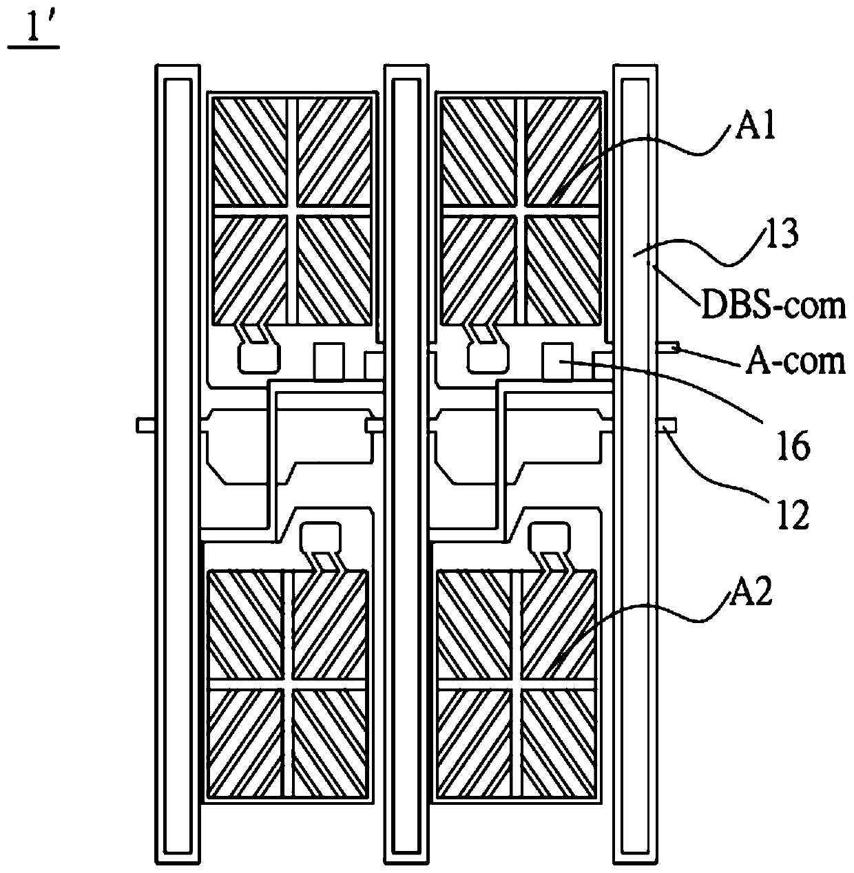
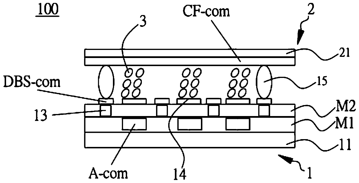
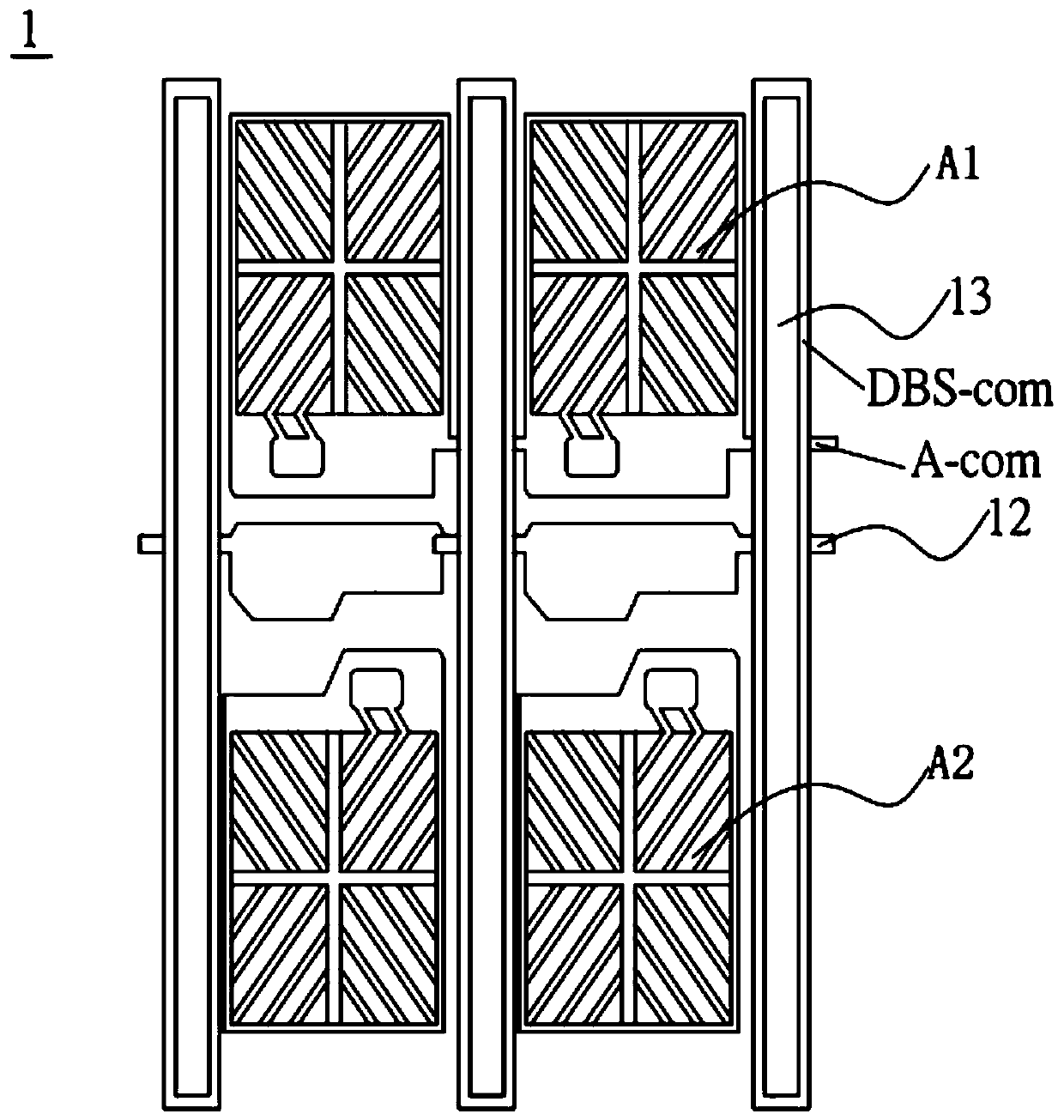
[0029] The following descriptions of the various embodiments refer to the accompanying drawings to illustrate specific embodiments in which the present disclosure may be practiced. The directional terms mentioned in this disclosure, such as [top], [bottom], [front], [back], [left], [right], [inside], [outside], [side], etc., are for reference only The orientation of the attached schema. Therefore, the directional terms used are used to explain and understand the present disclosure, but not to limit the present disclosure. In the figures, structurally similar elements are denoted by the same reference numerals.

[0030] This disclosure is aimed at the liquid crystal display panel in the prior art. When the liquid crystal display panel performs photo-matching, since the voltage of the common electrode line of the array substrate is not equal to the voltage of the common electrode layer of the color filter substrate, the voltage between the array substrate and the color filter s...


PUM


Abstract

The invention provides a liquid crystal display panel and a display device. The liquid crystal display panel comprises an array substrate, a color film substrate as well as a liquid crystal layer arranged between the array substrate and the color film substrate, wherein the array substrate comprises multiple scanning lines, multiple data lines, multiple pixel units defined by multiple scanning lines and multiple data lines as well as multiple DBS common electrode wires arrange above multiple data lines, partial DBS common electrode wires located at the periphery of the pixel units are electrically connected with a common electrode layer of the color film substrate, and partial DBS common electrode wires located at the inner sides of the pixel units are not connected with a common electrodewire of the array substrate, so that under the premise that an overall design architecture of the pixel units is not changed, voltage difference between the DBS common electrode wires and the commonelectrode layer of the color film substrate is reduced when the liquid crystal display panel performs light phase matching, burn caused by conductive foreign matters is avoided, foreign body sensationof the liquid crystal display panel is reduced, and yield is improved.

Description

technical field [0001] The disclosure relates to the field of display technology, and in particular to a liquid crystal display panel and a display device. Background technique [0002] Such as figure 1 Shown is a schematic top view of the structure of the existing array substrate 1' designed with Data Line BM Less (DBS) above the data lines. The existing liquid crystal display panel generally includes an array substrate 1', an array substrate 1' The color filter substrate (not shown in the figure) which is arranged relatively close to each other and the liquid crystal layer (not shown in the figure) arranged between the array substrate 1' and the color filter substrate, wherein the array substrate 1 'comprising a plurality of scanning lines 12 and a plurality of data lines 13, the gate lines 12 and the data lines 13 are intersected to define a plurality of pixel units, and pixel electrodes are arranged in the pixel units, and at the same time, the The array substrate uses...

Claims


Application Information

Patent Timeline
Patent Type & Authority Applications(China)
IPC IPC(8): G02F1/1343G02F1/1362G02F1/1368G02F1/1335
CPCG02F1/134309G02F1/13439G02F1/136286G02F1/1368G02F1/133514G02F1/133512G02F2201/121G02F1/136222G02F1/136218G02F1/13624G02F2201/122G02F2201/123
Inventor 蔡雪涛
Owner TCL CHINA STAR OPTOELECTRONICS TECH CO LTD
Why Eureka
Try Eureka