Film packaging method of stretchable organic photoelectric device

A technology for optoelectronic devices and thin film encapsulation, which is applied in the fields of electrical solid devices, electrical components, semiconductor devices, etc. It can solve the problems of reduced water and oxygen barrier performance, easy to produce cracks, etc., and achieves easy operation, improved packaging performance, and excellent conformality. retouching effect

Active Publication Date: 2019-08-02
FUZHOU UNIV
View PDF2 Cites 1 Cited by
  • Summary
  • Abstract
  • Description
  • Claims
  • Application Information

AI Technical Summary

Problems solved by technology

[0004] However, for stretchable devices, simply using atomic layer deposition to deposit dense inorganic materials on the substrate or the surface of the device or to prepare ino

Method used


Image

  • Film packaging method of stretchable organic photoelectric device
  • Film packaging method of stretchable organic photoelectric device

Examples


Embodiment Construction

[0029] In order to further understand the features and technical contents of the present invention, please refer to the detailed description and accompanying drawings of the present invention. The accompanying drawings are provided for reference and illustration only, and are not intended to limit the present invention.

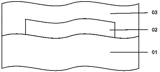
[0030] A thin film encapsulation method for stretchable organic optoelectronic devices, the thin film encapsulation structure prepared by it is sequentially provided with a stretchable organic polymer substrate 01 with high water and oxygen barrier performance, and a stretchable organic optoelectronic device 02 and inorganic / organic fusion overlapping thin film encapsulation layer 03 with high water and oxygen barrier properties, such as figure 1 Shown; Described stretchable organic optoelectronic device film encapsulation method comprises the steps:

[0031] S1 Place the stretchable organic polymer substrate in the reaction chamber of atomic layer deposition...


PUM


Abstract

The invention provides a film packaging method of a stretchable organic photoelectric device. A film packaging structure prepared by the method is provided with a stretchable organic polymer substratewith high water and oxygen obstruction performance, a stretchable organic photoelectric device and an inorganic/organic fused overlapped film packaging layer with high water and oxygen obstruction performance successively from bottom to top, inorganic/organic overlapped films are used in the high water and oxygen obstruction layer, the infiltration time of a precursor of atomic layer deposition in a reaction chamber is controlled, and an inorganic filling material is formed in the surfaces of the stretchable organic polymer substrate and the organic film layer to improve the water and oxygenobstruction performance thereof.

Description

technical field [0001] The invention relates to the field of flexible display technology, in particular to a film packaging method for stretchable organic photoelectric devices. Background technique [0002] For wearable devices and smart clothing, the future requires on-screen properties that can bend and stretch to match our bodies, and this requires ultra-flexible substrates. The flexible and stretchable substrate is generally an organic polymer material, and there are many holes and defects inside. The water vapor and oxygen in the air can easily penetrate the substrate and affect the display performance of the device. Atomic layer deposition is an excellent choice for modifying stretchable substrates due to its excellent three-dimensional conformality, large-area uniformity, sub-monolayer film thickness control, and low growth temperature. [0003] Atomic layer deposition technology is a method that pulses gas-phase precursors into the reaction chamber alternately, and...

Claims


Application Information

Patent Timeline
IPC IPC(8): H01L51/52H01L51/56
CPCH10K50/8445H10K50/84H10K71/00
Inventor 周雄图陈桂雄张永爱郭太良林志贤吴朝兴李福山杨尊先
Owner FUZHOU UNIV
Why Eureka
Try Eureka