Composition and organic optoelectronic element and its manufacturing method
A technology for optoelectronic components and manufacturing methods, which is applied in the fields of electrical components, semiconductor/solid-state device manufacturing, and electric-solid-state devices, etc., can solve problems such as large room for improvement, and achieve the effect of improving light extraction efficiency
- Summary
- Abstract
- Description
- Claims
- Application Information
AI Technical Summary
Problems solved by technology
Method used
Image
Examples
Embodiment 1
[0194] Fabrication of the charge transport layer
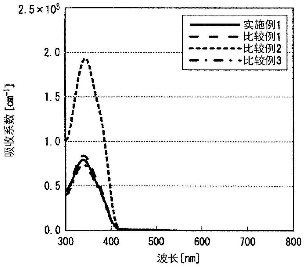
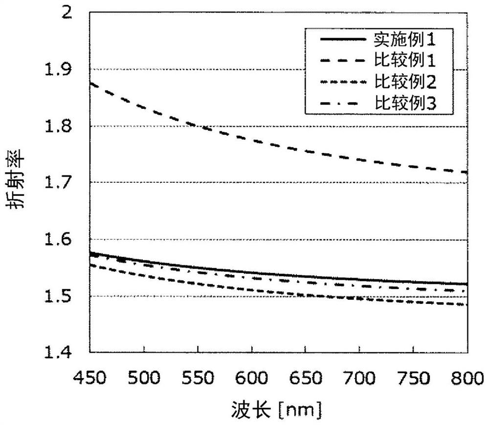
[0195] Two silicon substrates and one quartz substrate cut into about 2 cm square were ultrasonically cleaned with neutral detergent, acetone, and isopropanol, and then boiled and washed in isopropanol, and then treated with ozone to remove attachments. The substrates were respectively placed in a vacuum evaporation machine and vacuumed to a pressure of 10 -4 Pa or below, then use α-NPD and fluoropolymer A at a volume ratio of α-NPD and fluoropolymer A of 45:55, perform resistance heating in a vacuum evaporation machine, and perform co-evaporation, Thus, a charge transport layer having a thickness of about 100 nm was produced on each substrate. The total vapor deposition rate of the two materials was set to 0.2 nm / s. The surface roughness of the obtained charge transport layer was 0.33 nm.
[0196] Fabrication of elements for conductivity evaluation
[0197]A glass substrate on which a strip-shaped ITO (indium tin oxide) ...
Embodiment 2~9
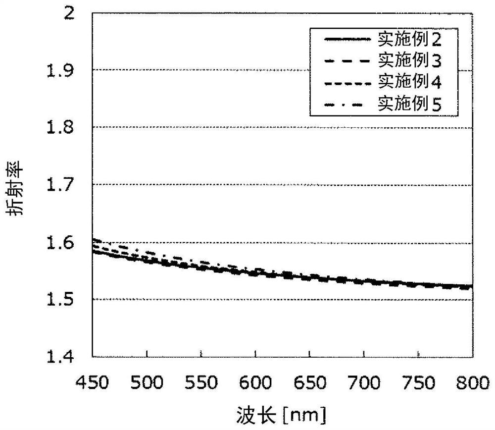
[0199] Except having used fluoropolymers B to J (except for D) instead of fluoropolymer A, it carried out similarly to Example 1, and produced the charge transport layer and the element for electroconductivity evaluation.
[0200] In addition, in Table 1, the name of the polymer used in each Example is described.
Embodiment 10
[0202] Except having used the fluorine-containing polymer K instead of the fluorine-containing polymer A, it carried out similarly to Example 1, and produced the charge transport layer and the element for conductivity evaluation.
PUM
| Property | Measurement | Unit |
|---|---|---|
| glass transition temperature | aaaaa | aaaaa |
| absorption coefficient | aaaaa | aaaaa |
| glass transition temperature | aaaaa | aaaaa |
Abstract
Description
Claims
Application Information


