BSI image sensor and manufacture thereof

An image sensor and back-illuminated technology, which is applied in semiconductor/solid-state device manufacturing, electric solid-state devices, semiconductor devices, etc., can solve problems affecting the quantum conversion efficiency of photoreceptors, production process mutual constraints, and device performance cannot be truly optimized.

Pending Publication Date: 2019-08-06
VISIONARY SEMICON INC
View PDF1 Cites 2 Cited by
  • Summary
  • Abstract
  • Description
  • Claims
  • Application Information

AI Technical Summary

Problems solved by technology

High-temperature process steps may seriously affect the minority carrier lifetime of the photosensitive region, thereby affecting the quantum conversion efficiency of the photoreceptor
In addition, the high-temperature process makes the photoreceptor and the pixel circuit need to be prepared at the same time, which prevents the production processes of the two parts of the device from being optimized separately. The production processes are mutually restricted, and finally the performance of the device cannot be truly optimized.
The current CMOS process is quite mature (reaching the 10nm technology node), but the optimized CMOS process often cannot be directly used in the preparation of image sensors (often using 60nm or even 90nm technology nodes)

Method used


Image

  • BSI image sensor and manufacture thereof
  • BSI image sensor and manufacture thereof
  • BSI image sensor and manufacture thereof

Examples


Embodiment Construction

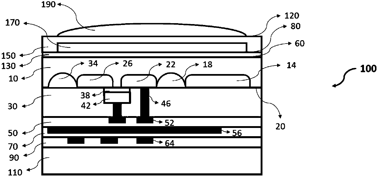
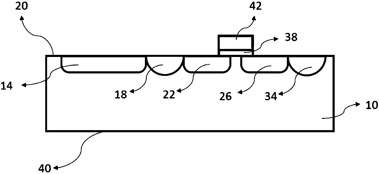
[0062] Embodiments of the present invention relate to a back-illuminated image sensor and a manufacturing method thereof according to an embodiment of the present invention, in particular, to a back-illuminated image sensor based on a heterojunction photoreceptor and a manufacturing method thereof according to an embodiment of the present invention method.

[0063] Referring to the drawings, the same or similar reference numerals are used throughout the various embodiments of the present invention to denote the same and similar elements in different drawings.

[0064]Since the present invention is about a back-illuminated image sensor based on heterojunction photoreceptors, the structure of the circuit part of the back-illuminated image sensor can basically adopt the prior art in the art (for example, U.S. Patent No. US7,875,948B2 ) in the known circuit structure and manufacturing process, in the following embodiments, the present invention only focuses on the differences and ...


PUM


Abstract

The invention provides a BSI image sensor including a photoreceptor portion and a circuit portion. The photoreceptor portion includes a micro-lens and a filter, wherein incident photons reach the BSIimage sensor by successively passing through the micro-lens and an optical filter; a transparent conductive film under the micro-lens and the optical filter, wherein the incident photons continue to pass through the transparent conductive film; and a first substrate disposed under the transparent conductive film, and used for capturing and detecting the received photons. The BSI image sensor is characterized in that a heterojunction is formed between the transparent conductive film and the first substrate. Additionally, the invention relates to a method for manufacturing a BSI image sensor ofthis type.

Description

technical field [0001] The invention relates to an image sensor with a back-illuminated structure. Specifically, the present invention relates to a back-illuminated image sensor based on a heterojunction photoreceptor and a preparation method thereof. Background technique [0002] CMOS image sensors are taking over the image sensor market dominated by CCD image sensors. In order to achieve high resolution with a limited-size image sensor, the size of each pixel in a CMOS image sensor continues to decrease, which makes the ratio of the photosensitive area to each pixel area (fill factor) particularly important. A low fill factor means that the metal circuit above the photoreceptor causes part of the photons to be reflected and lost before reaching the photoreceptor, which greatly affects the photosensitive efficiency of traditional image sensors, so a high fill factor is necessary for high photosensitivity. However, in order to continuously reduce system noise and increase ...

Claims


Application Information

Patent Timeline
Patent Type & Authority Applications(China)
IPC IPC(8): H01L27/146H01L21/70
CPCH01L27/14601H01L27/14683H01L21/70H01L27/1462H01L27/14627H01L27/14621H01L27/1463H01L27/14634H01L27/14689H01L27/1461H01L27/14643H01L27/1464H01L27/14685
Inventor 高朕
Owner VISIONARY SEMICON INC
Why Eureka
Try Eureka